


Home > Textbooks > Lessons In Electric Circuits > Vol. III - Semiconductors > Bipolar Junction Transistors > The Common-Base Amplifier
Chapter 4: BIPOLAR JUNCTION TRANSISTORS
The Common-Base Amplifier
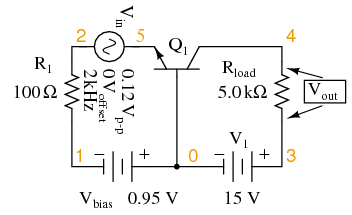
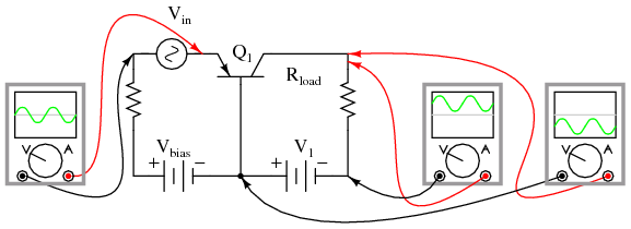
The final transistor amplifier configuration (Figure below) we need to study is the common-base. This configuration is more complex than the other two, and is less common due to its strange operating characteristics.
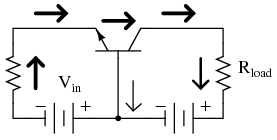
Common-base amplifier
It is called the common-base configuration because (DC power source aside), the signal source and the load share the base of the transistor as a common connection point shown in Figure below.
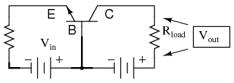
Common-base amplifier: Input between emitter and base, output between collector and base.
Perhaps the most striking characteristic of this configuration is that the input signal source must carry the full emitter current of the transistor, as indicated by the heavy arrows in the first illustration. As we know, the emitter current is greater than any other current in the transistor, being the sum of base and collector currents. In the last two amplifier configurations, the signal source was connected to the base lead of the transistor, thus handling the least current possible.
Because the input current exceeds all other currents in the circuit, including the output current, the current gain of this amplifier is actually less than 1 (notice how Rload is connected to the collector, thus carrying slightly less current than the signal source). In other words, it attenuates current rather than amplifying it. With common-emitter and common-collector amplifier configurations, the transistor parameter most closely associated with gain was β. In the common-base circuit, we follow another basic transistor parameter: the ratio between collector current and emitter current, which is a fraction always less than 1. This fractional value for any transistor is called the alpha ratio, or α ratio.
Since it obviously can't boost signal current, it only seems reasonable to expect it to boost signal voltage. A SPICE simulation of the circuit in Figure below will vindicate that assumption.
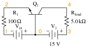
Common-base circuit for DC SPICE analysis.
|
common-base amplifier vin 0 1 r1 1 2 100 q1 4 0 2 mod1 v1 3 0 dc 15 rload 3 4 5k .model mod1 npn .dc vin 0.6 1.2 .02 .plot dc v(3,4) .end |
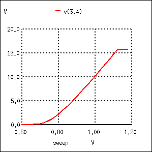
Common-base amplifier DC transfer function.
Notice in Figure above that the output voltage goes from practically nothing (cutoff) to 15.75 volts (saturation) with the input voltage being swept over a range of 0.6 volts to 1.2 volts. In fact, the output voltage plot doesn't show a rise until about 0.7 volts at the input, and cuts off (flattens) at about 1.12 volts input. This represents a rather large voltage gain with an output voltage span of 15.75 volts and an input voltage span of only 0.42 volts: a gain ratio of 37.5, or 31.48 dB. Notice also how the output voltage (measured across Rload) actually exceeds the power supply (15 volts) at saturation, due to the series-aiding effect of the input voltage source.
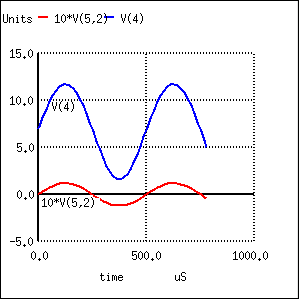
A second set of SPICE analyses (circuit in Figure below) with an AC signal source (and DC bias voltage) tells the same story: a high voltage gain
Common-base circuit for SPICE AC analysis.
As you can see, the input and output waveforms in Figure below are in phase with each other. This tells us that the common-base amplifier is non-inverting.
|
common-base amplifier
vin 5 2 sin (0 0.12 2000 0 0)
vbias 0 1  dc 0.95
r1 2 1 100
q1 4 0 5 mod1
v1 3 0 dc 15
rload 3 4 5k
.model mod1 npn
.tran 0.02m 0.78m
.plot tran v(5,2) v(4)
.end
|
The AC SPICE analysis in Table below at a single frequency of 2 kHz provides input and output voltages for gain calculation.
Common-base AC analysis at 2 kHz— netlist followed by output.
common-base amplifier
vin 5 2  ac 0.1 sin
vbias 0 1  dc 0.95
r1 2 1 100
q1 4 0 5 mod1
v1 3 0 dc 15
rload 3 4 5k
.model mod1 npn
.ac dec 1 2000 2000
.print ac vm(5,2) vm(4,3)
.end

frequency       mag(v(5,2))     mag(v(4,3))
--------------------------------------------
0.000000e+00    1.000000e-01    4.273864e+00
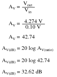
Voltage figures from the second analysis (Table above) show a voltage gain of 42.74 (4.274 V / 0.1 V), or 32.617 dB:
Here's another view of the circuit in Figure below, summarizing the phase relations and DC offsets of various signals in the circuit just simulated.
Phase relationships and offsets for NPN common base amplifier.
. . . and for a PNP transistor: Figure below.
Phase relationships and offsets for PNP common base amplifier.
Predicting voltage gain for the common-base amplifier configuration is quite difficult, and involves approximations of transistor behavior that are difficult to measure directly. Unlike the other amplifier configurations, where voltage gain was either set by the ratio of two resistors (common-emitter), or fixed at an unchangeable value (common-collector), the voltage gain of the common-base amplifier depends largely on the amount of DC bias on the input signal. As it turns out, the internal transistor resistance between emitter and base plays a major role in determining voltage gain, and this resistance changes with different levels of current through the emitter.
While this phenomenon is difficult to explain, it is rather easy to demonstrate through the use of computer simulation. What I'm going to do here is run several SPICE simulations on a common-base amplifier circuit (Figure previous), changing the DC bias voltage slightly (vbias in Figure below ) while keeping the AC signal amplitude and all other circuit parameters constant. As the voltage gain changes from one simulation to another, different output voltage amplitudes will be noted.
Although these analyses will all be conducted in the “transfer function” mode, each was first “proofed” in the transient analysis mode (voltage plotted over time) to ensure that the entire wave was being faithfully reproduced and not “clipped” due to improper biasing. See “*.tran 0.02m 0.78m” in Figure below, the “commented out” transient analysis statement. Gain calculations cannot be based on waveforms that are distorted. SPICE can calculate the small signal DC gain for us with the “.tf v(4) vin” statement. The output is v(4) and the input as vin.
common-base amp vbias=0.85V vin 5 2 sin (0 0.12 2000 0 0) vbias 0 1 dc 0.85 r1 2 1 100 q1 4 0 5 mod1 v1 3 0 dc 15 rload 3 4 5k .model mod1 npn *.tran 0.02m 0.78m .tf v(4) vin .end |
common-base amp current gain Iin 55 5 0A vin 55 2 sin (0 0.12 2000 0 0) vbias 0 1 dc 0.8753 r1 2 1 100 q1 4 0 5 mod1 v1 3 0 dc 15 rload 3 4 5k .model mod1 npn *.tran 0.02m 0.78m .tf I(v1) Iin .end Transfer function information: transfer function = 9.900990e-01 iin input impedance = 9.900923e+11 v1 output impedance = 1.000000e+20 |
SPICE net list: Common-base, transfer function (voltage gain) for various DC bias voltages. SPICE net list: Common-base amp current gain; Note .tf v(4) vin statement. Transfer function for DC current gain I(vin)/Iin; Note .tf I(vin) Iin statement.
At the command line, spice -b filename.cir produces a printed output due to the .tf statement: transfer_function, output_impedance, and input_impedance. The abbreviated output listing is from runs with vbias at 0.85, 0.90, 0.95, 1.00 V as recorded in Table below.
SPICE output: Common-base transfer function.
Circuit: common-base amp vbias=0.85V
transfer_function = 3.756565e+01
output_impedance_at_v(4) = 5.000000e+03
vin#input_impedance = 1.317825e+02

Circuit: common-base amp vbias=0.8753V Ic=1 mA
Transfer function information:
transfer_function = 3.942567e+01
output_impedance_at_v(4) = 5.000000e+03
vin#input_impedance = 1.255653e+02

Circuit: common-base amp vbias=0.9V
transfer_function = 4.079542e+01
output_impedance_at_v(4) = 5.000000e+03
vin#input_impedance = 1.213493e+02

Circuit: common-base amp vbias=0.95V
transfer_function = 4.273864e+01
output_impedance_at_v(4) = 5.000000e+03
vin#input_impedance = 1.158318e+02

Circuit: common-base amp vbias=1.00V
transfer_function = 4.401137e+01
output_impedance_at_v(4) = 5.000000e+03
vin#input_impedance = 1.124822e+02
A trend should be evident in Table above. With increases in DC bias voltage, voltage gain (transfer_function) increases as well. We can see that the voltage gain is increasing because each subsequent simulation (vbias= 0.85, 0.8753, 0.90, 0.95, 1.00 V) produces greater gain (transfer_function= 37.6, 39.4 40.8, 42.7, 44.0), respectively. The changes are largely due to minuscule variations in bias voltage.
The last three lines of Table above(right) show the I(v1)/Iin current gain of 0.99. (The last two lines look invalid.) This makes sense for β=100; α= β/(β+1), α=0.99=100/(100-1). The combination of low current gain (always less than 1) and somewhat unpredictable voltage gain conspire against the common-base design, relegating it to few practical applications.
Those few applications include radio frequency amplifiers. The grounded base helps shield the input at the emitter from the collector output, preventing instability in RF amplifiers. The common base configuration is usable at higher frequencies than common emitter or common collector. See “Class C common-base 750 mW RF power amplifier” Ch 9 . For a more elaborate circuit see “Class A common-base small-signal high gain amplifier” Ch 9.
- REVIEW:
- Common-base transistor amplifiers are so-called because the input and output voltage points share the base lead of the transistor in common with each other, not considering any power supplies.
- The current gain of a common-base amplifier is always less than 1. The voltage gain is a function of input and output resistances, and also the internal resistance of the emitter-base junction, which is subject to change with variations in DC bias voltage. Suffice to say that the voltage gain of a common-base amplifier can be very high.
- The ratio of a transistor's collector current to emitter current is called α. The α value for any transistor is always less than unity, or in other words, less than 1.


Related Content:
Circuits: Common-base amplifier.