


Home > Textbooks > Lessons In Electric Circuits > Vol. III - Semiconductors > Junction Field-Effect Transistors > The Transistor as a Switch
Chapter 5: JUNCTION FIELD-EFFECT TRANSISTORS
The Transistor as a Switch
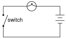
Like its bipolar cousin, the field-effect transistor may be used as an on/off switch controlling electrical power to a load. Let's begin our investigation of the JFET as a switch with our familiar switch/lamp circuit:
Remembering that the controlled current in a JFET flows between source and drain, we substitute the source and drain connections of a JFET for the two ends of the switch in the above circuit:
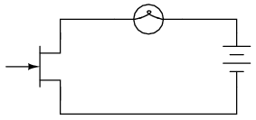
If you haven't noticed by now, the source and drain connections on a JFET look identical on the schematic symbol. Unlike the bipolar junction transistor where the emitter is clearly distinguished from the collector by the arrowhead, a JFET's source and drain lines both run perpendicular into the bar representing the semiconductor channel. This is no accident, as the source and drain lines of a JFET are often interchangeable in practice! In other words, JFETs are usually able to handle channel current in either direction, from source to drain or from drain to source.
Now all we need in the circuit is a way to control the JFET's conduction. With zero applied voltage between gate and source, the JFET's channel will be "open," allowing full current to the lamp. In order to turn the lamp off, we will need to connect another source of DC voltage between the gate and source connections of the JFET like this:
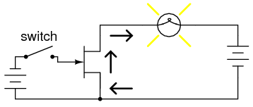
Closing this switch will "pinch off" the JFET's channel, thus forcing it into cutoff and turning the lamp off:
Note that there is no current going through the gate. As a reverse-biased PN junction, it firmly opposes the flow of any electrons through it. As a voltage-controlled device, the JFET requires negligible input current. This is an advantageous trait of the JFET over the bipolar transistor: there is virtually zero power required of the controlling signal.
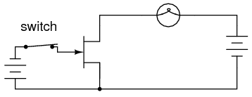
Opening the control switch again should disconnect the reverse-biasing DC voltage from the gate, thus allowing the transistor to turn back on. Ideally, anyway, this is how it works. In practice this may not work at all:
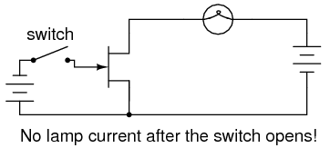
Why is this? Why doesn't the JFET's channel open up again and allow lamp current through like it did before with no voltage applied between gate and source? The answer lies in the operation of the reverse-biased gate-source junction. The depletion region within that junction acts as an insulating barrier separating gate from source. As such, it possesses a certain amount of capacitance capable of storing an electric charge potential. After this junction has been forcibly reverse-biased by the application of an external voltage, it will tend to hold that reverse-biasing voltage as a stored charge even after the source of that voltage has been disconnected. What is needed to turn the JFET on again is to bleed off that stored charge between the gate and source through a resistor:
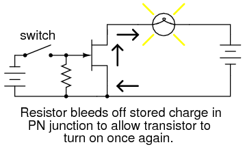
This resistor's value is not very important. The capacitance of the JFET's gate-source junction is very small, and so even a rather high-value bleed resistor creates a fast RC time constant, allowing the transistor to resume conduction with little delay once the switch is opened.
Like the bipolar transistor, it matters little where or what the controlling voltage comes from. We could use a solar cell, thermocouple, or any other sort of voltage-generating device to supply the voltage controlling the JFET's conduction. All that is required of a voltage source for JFET switch operation is sufficient voltage to achieve pinch-off of the JFET channel. This level is usually in the realm of a few volts DC, and is termed the pinch-off or cutoff voltage. The exact pinch-off voltage for any given JFET is a function of its unique design, and is not a universal figure like 0.7 volts is for a silicon BJT's base-emitter junction voltage.
- REVIEW:
- Field-effect transistors control the current between source and drain connections by a voltage applied between the gate and source. In a junction field-effect transistor (JFET), there is a PN junction between the gate and source which is normally reverse-biased for control of source-drain current.
- JFETs are normally-on (normally-saturated) devices. The application of a reverse-biasing voltage between gate and source causes the depletion region of that junction to expand, thereby "pinching off" the channel between source and drain through which the controlled current travels.
- It may be necessary to attach a "bleed-off" resistor between gate and source to discharge the stored charge built up across the junction's natural capacitance when the controlling voltage is removed. Otherwise, a charge may remain to keep the JFET in cutoff mode even after the voltage source has been disconnected.


