


Home > Textbooks > Lessons In Electric Circuits > Vol. III - Semiconductors > Thyristors > The Unijunction Transistor (UJT)
Chapter 7: THYRISTORS
The Unijunction Transistor (UJT)
Unijunction transistor: Although a unijunction transistor is not a thyristor, this device can trigger larger thyristors with a pulse at base B1. A unijunction transistor is composed of a bar of N-type silicon having a P-type connection in the middle. See Figure below(a). The connections at the ends of the bar are known as bases B1 and B2; the P-type mid-point is the emitter. With the emitter disconnected, the total resistance RBBO, a datasheet item, is the sum of RB1 and RB2 as shown in Figure below(b). RBBO ranges from 4-12kΩ for different device types. The intrinsic standoff ratio η is the ratio of RB1 to RBBO. It varies from 0.4 to 0.8 for different devices. The schematic symbol is Figure below(c).
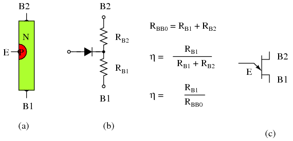
Unijunction transistor: (a) Construction, (b) Model, (c) Symbol
The Unijunction emitter current vs voltage characteristic curve (Figure below(a)) shows that as VE increases, current IE increases up IP at the peak point. Beyond the peak point, current increases as voltage decreases in the negative resistance region. The voltage reaches a minimum at the valley point. The resistance of RB1, the saturation resistance is lowest at the valley point.
IP and IV, are datasheet parameters; For a 2n2647, IP and IV are 2µA and 4mA, respectively. [5] VP is the voltage drop across RB1 plus a 0.7V diode drop; see Figure below(b). VV is estimated to be approximately 10% of VBB.
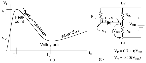
Unijunction transistor: (a) emitter characteristic curve, (b) model for VP .
The relaxation oscillator in Figure below is an application of the unijunction oscillator. RE charges CE until the peak point. The unijunction emitter terminal has no effect on the capacitor until this point is reached. Once the capacitor voltage, VE, reaches the peak voltage point VP, the lowered emitter-base1 E-B1 resistance quickly discharges the capacitor. Once the capacitor discharges below the valley point VV, the E-RB1 resistance reverts back to high resistance, and the capacitor is free to charge again.
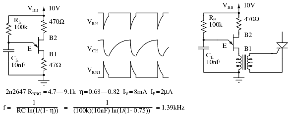
Unijunction transistor relaxation oscillator and waveforms. Oscillator drives SCR.
During capacitor discharge through the E-B1 saturation resistance, a pulse may be seen on the external B1 and B2 load resistors, Figure above. The load resistor at B1 needs to be low to not affect the discharge time. The external resistor at B2 is optional. It may be replaced by a short circuit. The approximate frequency is given by 1/f = T = RC. A more accurate expression for frequency is given in Figure above.
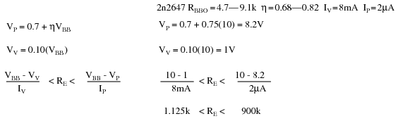
The charging resistor RE must fall within certain limits. It must be small enough to allow IP to flow based on the VBB supply less VP. It must be large enough to supply IV based on the VBB supply less VV. [6] The equations and an example for a 2n2647:
Programmable Unijunction Transistor (PUT): Although the unijunction transistor is listed as obsolete (read expensive if obtainable), the programmable unijunction transistor is alive and well. It is inexpensive and in production. Though it serves a function similar to the unijunction transistor, the PUT is a three terminal thyristor. The PUT shares the four-layer structure typical of thyristors shown in Figure below. Note that the gate, an N-type layer near the anode, is known as an “anode gate”. Moreover, the gate lead on the schematic symbol is attached to the anode end of the symbol.
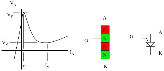
Programmable unijunction transistor: Characteristic curve, internal construction, schematic symbol.
The characteristic curve for the programmable unijunction transistor in Figure above is similar to that of the unijunction transistor. This is a plot of anode current IA versus anode voltage VA. The gate lead voltage sets, programs, the peak anode voltage VP. As anode current inceases, voltage increases up to the peak point. Thereafter, increasing current results in decreasing voltage, down to the valley point.
The PUT equivalent of the unijunction transistor is shown in Figure below. External PUT resistors R1 and R2 replace unijunction transistor internal resistors RB1 and RB2, respectively. These resistors allow the calculation of the intrinsic standoff ratio η.
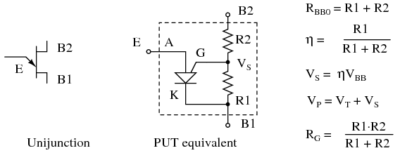
PUT equivalent of unijunction transistor
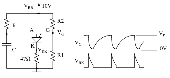
Figure below shows the PUT version of the unijunction relaxation oscillator Figure previous. Resistor R charges the capacitor until the peak point, Figure previous, then heavy conduction moves the operating point down the negative resistance slope to the valley point. A current spike flows through the cathode during capacitor discharge, developing a voltage spike across the cathode resistors. After capacitor discharge, the operating point resets back to the slope up to the peak point.
PUT relaxation oscillator
Problem: What is the range of suitable values for R in Figure above, a relaxation oscillator? The charging resistor must be small enough to supply enough current to raise the anode to VP the peak point (Figure previous) while charging the capacitor. Once VP is reached, anode voltage decreases as current increases (negative resistance), which moves the operating point to the valley. It is the job of the capacitor to supply the valley current IV. Once it is discharged, the operating point resets back to the upward slope to the peak point. The resistor must be large enough so that it will never supply the high valley current IP. If the charging resistor ever could supply that much current, the resistor would supply the valley current after the capacitor was discharged and the operating point would never reset back to the high resistance condition to the left of the peak point.
We select the same VBB=10V used for the unijunction transistor example. We select values of R1 and R2 so that η is about 2/3. We calculate η and VS. The parallel equivalent of R1, R2 is RG, which is only used to make selections from Table below. Along with VS=10, the closest value to our 6.3, we find VT=0.6V, in Table below and calculate VP.
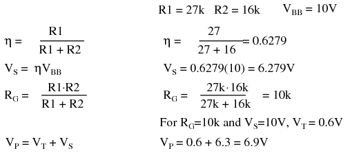
We also find IP and IV, the peak and valley currents, respectively in Table below. We still need VV, the valley voltage. We used 10% of VBB= 1V, in the previous unijunction example. Consulting the datasheet, we find the forward voltage VF=0.8V at IF=50mA. The valley current IV=70µA is much less than IF=50mA. Therefore, VV must be less than VF=0.8V. How much less? To be safe we set VV=0V. This will raise the lower limit on the resistor range a little.
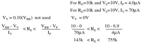
Choosing R > 143k guarantees that the operating point can reset from the valley point after capacitor discharge. R < 755k allows charging up to VP at the peak point.
Selected 2n6027 PUT parameters, adapted from 2n6027 datasheet. [4]
| Parameter | Conditions | min | typical | max | units |
|---|---|---|---|---|---|
| VT | V | ||||
| VS=10V, RG=1Meg | 0.2 | 0.7 | 1.6 | ||
| VS=10V, RG=10k | 0.2 | 0.35 | 0.6 | ||
| IP | µA | ||||
| VS=10V, RG=1Meg | - | 1.25 | 2.0 | ||
| VS=10V, RG=10k | - | 4.0 | 5.0 | ||
| IV | µA | ||||
| VS=10V, RG=1Meg | - | 18 | 50 | ||
| VS=10V, RG=10k | 70 | 150 | - | ||
| VS=10V, RG=200Ω | 1500 | - | - | ||
| VF | IF=50mA | - | 0.8 | 1.5 | V |
Figure below show the PUT relaxation oscillator with the final resistor values. A practical application of a PUT triggering an SCR is also shown. This circuit needs a VBB unfiltered supply (not shown) divided down from the bridge rectifier to reset the relaxation oscillator after each power zero crossing. The variable resistor should have a minimum resistor in series with it to prevent a low pot setting from hanging at the valley point.
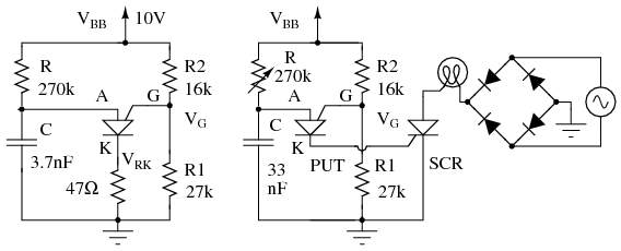
PUT relaxation oscillator with component values. PUT drives SCR lamp dimmer.
PUT timing circuits are said to be usable to 10kHz. If a linear ramp is required instead of an exponential ramp, replace the charging resistor with a constant current source such as a FET based constant current diode. A substitute PUT may be built from a PNP and NPN silicon transistor as shown for the SCS equivalent circuit in Figure below by omitting the cathode gate and using the anode gate.
- REVIEW:
- A unijunction transistor consists of two bases (B1, B2) attached to a resistive bar of silicon, and an emitter in the center. The E-B1 junction has negative resistance properties; it can switch between high and low resistance.
- A PUT (programmable unijunction transistor) is a 3-terminal 4-layer thyristor acting like a unijunction transistor. An external resistor network “programs” η.
- The intrinsic standoff ratio is η=R1/(R1+R2) for a PUT; substitute RB1 and RB2, respectively, for a unijunction transistor. The trigger voltage is determined by η.
- Unijunction transistors and programmable unijunction transistors are applied to oscillators, timing circuits, and thyristor triggering.


