


Home > Textbooks > Selected Circuits > Bipolar Junction Transistors > Signal Gate >
Bipolar Junction Transistors
Signal Gate
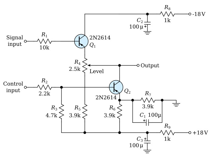
This circuit is composed of an emitter follower whose output is shunted by a common emitter amplifier. The common emitter amplifier is turned on and off by an external control signal. When this stage is off, it permits the input signal to pass through the gate circuit.
The signal to be gated is fed into the Signal input and through R1 to the base of the emitter follower Q1. The emitter of Q1 is connected through R4 and R5 to the positive supply in order to permit the output signal to swing both positive and negative. R4 acts as an amplitude control to permit setting the level of the signal.
Q2 is connected across the output from the emitter follower. R7 and R6 form a voltage divider between the +18V and ground, holding the emitter at a slight positive voltage (about 5V when not conducting). The base of Q2 is held slightly positive by R3. The gate control signal is fed into the Control input and through R2 to the base of Q2. When this signal is zero, the positive potential on the base of Q2 prevents the transistor from conducting. When the transistor (Q2) is turned off, it represents a high impedance between the output and ground.
When the control input becomes negative, the input current overcomes the positive bias at the base of Q2 causing it to conduct and saturate. With Q2 turned full on, the signal at the arm of R4 is shorted to ground through Q2 and C1. R8, C2, and R9, C3 form filtering networks.
