


Home > Textbooks > Selected Circuits > Logic Gates > Dwell-Time Gate >
Logic Gates
Dwell-Time Gate
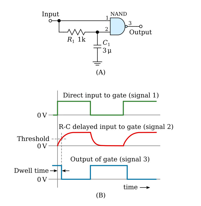
The purpose of the dwell-time gate is to provide a time delay, or dwell time, between the leading edge of the input and trailing edge of the output.
View B of the figure above shows the typical inputs and output of a logic gate used in the dwell-time circuitry. One input to the NAND gate (1) comes directly from the input source. The other input to the gate (2) is the same as the first but is fed through an R-C delay network (R1 and C1). The gate requires two high-level input signals to be changed to low-level output. This does not occur until the R-C network voltage reaches the threshold level of the gate, as shown in view B of the figure. The dwell time is thus determined by the time constant of the R-C network. A dwell-time duration of 3 ms is used. The trailing edges of the input waveform are not affected by the dwell-time circuitry, since as soon as the direct input to the dwell-time gate changes state, the gate output also changes state.
