


Home > Textbooks > Solid-State Devices > Semiconductor Diodes > Construction >
SEMICONDUCTOR DIODES
Construction
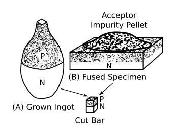
Merely pressing together a section of P material and a section of N material, however, is not sufficient to produce a rectifying junction. The semiconductor should be in one piece to form a proper PN junction, but divided into a P-type impurity region and an N-type impurity region. This can be done in various ways. One way is to mix P-type and N-type impurities into a single crystal during the manufacturing process. By so doing, a P-region is grown over part of a semiconductor's length and N-region is grown over the other part. This is called a GROWN junction and is illustrated in view A of the figure below. Another way to produce a PN junction is to melt one type of impurity into a semiconductor of the opposite type impurity. For example, a pellet of acceptor impurity is placed on a wafer of N-type germanium and heated. Under controlled temperature conditions, the acceptor impurity fuses into the wafer to form a P-region within it, as shown in view B of the figure below. This type of junction is known as an ALLOY or FUSED-ALLOY junction, and it is one of the most commonly used junctions.
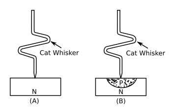
In the figure below, a POINT-CONTACT type of construction is shown. It consists of a fine metal wire, called a cat whisker, that makes contact with a small area on the surface of an N-type semiconductor as shown in view A of the figure. The PN union is formed in this process by momentarily applying a high-surge current to the wire and the N-type semiconductor. The heat generated by this current converts the material nearest the point of contact to a P-type material (view B).
Still another process is to heat a section of semiconductor material to near melting and then diffuse impurity atoms into a surface layer. Regardless of the process, the object is to have a perfect bond everywhere along the union (interface) between P and N materials. Proper contact along the union is important because, as we will see later, the union (junction or interface) is the rectifying agent in the diode.


