


Home > Textbooks > Selected Circuits > Switches > Ultrafast Sampling Switch >
Switches
Ultrafast Sampling Switch
Probably the single most important requirement for the sampling switch is high switching speed. Switching speed of the MOSFET is very fast but is highly dependent upon the circuit in which it is used. In order to obtain turn-on times as short as 50 ns, careful consideration must be given to all circuit parameters, especially source and load impedances.
The MOSFET used in the switching circuit is 3N163. This is a p-channel type MOSFET with an n-type substrate (bulk). For zero gate voltages no current will flow from source to drain. The application of a negative gate voltage of sufficient amplitude draws holes into the region below the gate so that this channel region changes from a n-type to a p-type and provides a source to drain conduction path. As the flow of current is made possible (enhanced) the MOSFET described is properly called an enhancement-mode device. The off resistance of the 3N163 MOSFET exceeds five gigaohms (5 × 10⁹ Ω). The on-state resistance is typically about 100 Ω.
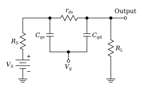
The gate is completely isolated from the rest of the device by the metal oxide layer. Therefore the input impedance at the gate is that of a capacitor only. This amounts to about 3 pF. The capacitance from gate to drain Cgd is about 0.7 pF. Although this capacitance is very small it represents a major disadvantage of the MOSFET as an analog gate at high gate drive frequencies. Due to Cgd and any stray capacitance present, a portion of the gate drive signal is coupled into the load circuit and causes a voltage spike to appear across the load resistance RL each time the gate drive signal changes state as Cgd and RL form a differentiating network. This can be better understood by referring to the equivalent circuit shown in the figure below.
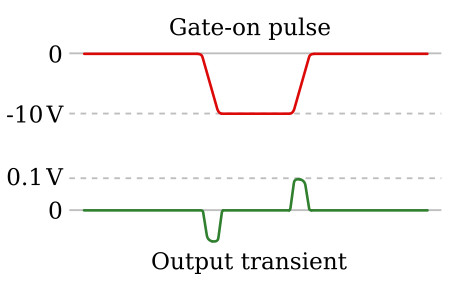
The induced transients can be reduced by using a gate-on signal with poor rise and fall times. Unfortunately this solution cannot be used, as very fast switching speeds are desirable. Low source and drain impedances will reduce the amplitude of these spikes. For this reason and to reduce the input and output time constants (and thus increase switching speeds) relatively low source and load impedances must be used. In practice, the induced transients can be reduced but not eliminated.
The interelectrode capacitances of the MOSFET affect the operation in sampling switch circuits at high signal frequencies. As shown in the figure above, Cgd and Cgs together form a series capacitance in parallel with the drain to source impedance rds. When the reactance of this effective capacitance becomes significantly lower than the MOSFET off-state resistance the input signal can be transferred into the load circuit even when no gate-on pulse is present. This problem is of little concern as the signal frequency in the application is low. It would be a problem at signal frequencies in excess of several megahertz.
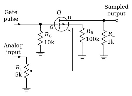
The schematic of the ultrafast sampling switch is shown above. In the absence of a negative gate-on pulse from the gate-control generator, Q represents a series resistance of 5 gigaohms between the input and the output RL. The variable resistor R1 is a gain adjust control to compensate for variations in MOSFET on-state resistance. A typical gate-on signal and transient induced in the output (across RL) for zero input voltage is shown in the figure below.
Useful link: 3N163 datasheet (pdf)
