Home > Textbooks > Solid-State Devices > Special Devices > Metal Oxide Semiconductor Field-Effect Transistors >
SPECIAL DEVICES
Metal Oxide Semiconductor Field-Effect Transistors
A second type of field-effect transistor has been introduced in recent years that has some advantages over the JFET. This device is the metal oxide semiconductor field effect transistor (MOSFET). The MOSFET has an even higher input impedance than the JFET (10 to 100 million megohms). Therefore, the MOSFET is even less of a load on preceding circuits. The extremely high input impedance, combined with a high gain factor, makes the MOSFET a highly efficient input device for RF/IF amplifiers and mixers and for many types of test equipment.
The MOSFET is normally constructed so that it operates in one of two basic modes: the depletion mode or the enhancement mode. The depletion mode MOSFET has a heavily doped channel and uses reverse bias on the gate to cause a depletion of current carriers in the channel. The JFET also operates in this manner. The enhancement mode MOSFET has a lightly doped channel and uses forward bias to enhance the current carriers in the channel. A MOSFET can be constructed that will operate in either mode depending upon what type of bias is applied, thus allowing a greater range of input signals.
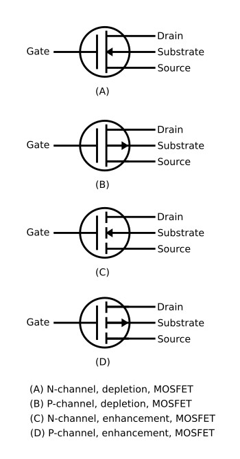
In addition to the two basic modes of operation, the MOSFET, like the JFET, is of either the P-channel type or the N-channel type. Each type has four elements: gate, source, drain, and substrate. The schematic symbols for the four basic variations of the MOSFET are shown in views A, B, C, and D of the figure below.
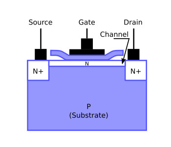
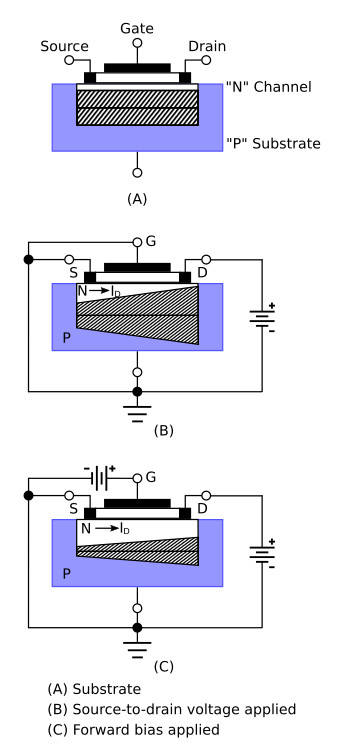
The construction of an N-channel MOSFET is shown in the figure below. Heavily doped N-type regions (indicated by the N+) are diffused into a P-type substrate or base. A channel of regular N-type material is diffused between the heavily doped N-type regions. A metal oxide insulating layer is then formed over the channel, and a metal gate layer is deposited over the insulating layer. There is no electrical connection between the gate and the rest of the device. This construction method results in the extremely high input impedance of the MOSFET. Another common name for the device, derived from the construction method, is the insulated gate field effect transistor (IGFET).
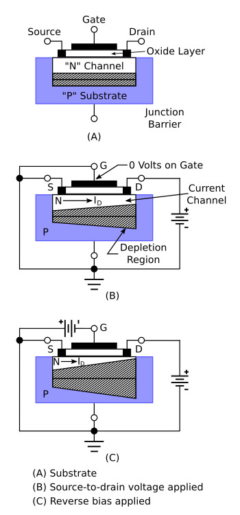
The operation of the MOSFET, or IGFET, is basically the same as the operation of the JFET. The current flow between the source and drain can be controlled by using either of two methods or by using a combination of the two methods. In one method the drain voltage controls the current when the gate potential is at zero volts. A voltage is applied to the gate in the second method. An electric field is formed by the gate voltage that affects the current flow in the channel by either depleting or enhancing the number of current carriers available. As previously stated, a reverse bias applied to the gate depletes the carriers, and a forward bias enhances the carriers. The polarity of the voltages required to forward or reverse bias a MOSFET depends upon whether it is of the P-channel type or the N-channel type. The effects of reverse-bias voltage on a MOSFET designed to operate in the depletion mode are illustrated in views A, B, and C of the figure below. The amount of reverse bias applied has a direct effect on the width of the current channel and, thus, the amount of drain current (Id).
The figure below illustrates the effect of forward bias on an enhancement mode N-channel MOSFET. In this case, a positive voltage applied to the gate increases the width of the current channel and the amount of drain current (Id).
Another type of MOSFET is the induced-channel type MOSFET. Unlike the MOSFETs discussed so far, the induced-channel type has no actual channel between the source and the drain. The induced channel MOSFET is constructed by making the channel of the same type material as the substrate, or the opposite of the source and the drain material. As shown in the figure below, the source and the drain are of P-type material, and the channel and the substrate are of N-type material.
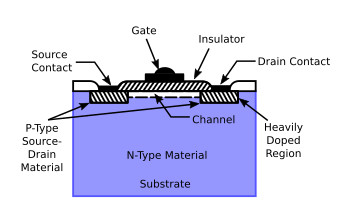
The induced-channel MOSFET is caused to conduct from source to drain by the electric field that is created when a voltage is applied to the gate. For example, assume that a negative voltage is applied to the MOSFET in the figure above. The effect of the negative voltage modifies the conditions in the substrate material. As the gate builds a negative charge, free electrons are repelled, forming a depletion region. Once a certain level of depletion has occurred (determined by the composition of the substrate material), any additional gate bias attracts positive holes to the surface of the substrate. When enough holes have accumulated at the surface channel area, the channel changes from an N-type material to a P-type material, since it now has more positive carriers than negative carriers. At this point the channel is considered to be to inverted, and the two P-type regions at the source and the drain are now connected by a P-type inversion layer or channel. As with the MOSFET, the gate signal determines the amount of current flow through the channel as long as the source and drain voltages remain constant. When the gate voltage is at zero, essentially no current flows since a gate voltage is required to form a channel.
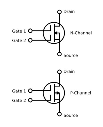
The MOSFETs discussed up to this point have single-gate MOSFETs. Another type of MOSFET, the dual-gate type, is shown in the figure below. Because the substrate has been connected directly to the source terminal, the dual-gate MOSFET still has only four leads: one each for source and drain, and two for the gates. Either gate can control conduction independently, making this type of MOSFET a truly versatile device.
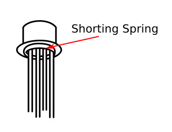
One problem with both the single- and dual-gate MOSFET is that the oxide layer between gate and channel can be destroyed very easily by ordinary static electricity. Replacement MOSFETs come packaged with their leads shorted together by a special wire loop or spring to avoid accidental damage. The rule to remember with these shorting springs is that they must not be removed until after the MOSFET has been soldered or plugged into a circuit. One such spring is shown in the figure below.