


Home > Textbooks > Solid-State Devices > Bipolar Transistors > Construction >
BIPOLAR TRANSISTORS
Construction
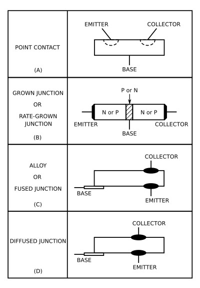
The very first transistors were known as point-contact transistors. Their construction is similar to the construction of the point-contact diode. The difference, of course, is that the point-contact transistor has two P or N regions formed instead of one. Each of the two regions constitutes an electrode (element) of the transistor. One is named the emitter and the other is named the collector, as shown in the figure above, view A.
Point-contact transistors are now practically obsolete. They have been replaced by junction transistors, which are superior to point-contact transistors in nearly all respects. The junction transistor generates less noise, handles more power, provides higher current and voltage gains, and can be mass-produced more cheaply than the point-contact transistor. Junction transistors are manufactured in much the same manner as the PN junction diode discussed earlier. However, when the PNP or NPN material is grown (view B), the impurity mixing process must be reversed twice to obtain the two junctions required in a transistor. Likewise, when the alloy-junction (view C) or the diffused-junction (view D) process is used, two junctions must also be created within the crystal.
Although there are numerous ways to manufacture transistors, one of the most important parts of any manufacturing process is quality control. Without good quality control, many transistors would prove unreliable because the construction and processing of a transistor govern its thermal ratings, stability, and electrical characteristics. Even though there are many variations in the transistor manufacturing processes, certain structural techniques, which yield good reliability and long life, are common to all processes: (1) Wire leads are connected to each semiconductor electrode; (2) the crystal is specially mounted to protect it against mechanical damage; and (3) the unit is sealed to prevent harmful contamination of the crystal.


