


Home > Textbooks > Basic Electronics > Bipolar Junction Transistors > Transistor as a Switch >
Bipolar Junction Transistors
Transistor as a Switch
An ideal switch is characterized by an infinite resistance when it is open, zero resistance when it is closed, and an input by which it can be opened or closed. Transistors can be used as switches. The advantages which transistor switches offer over mechanical switches are that there are no moving or wearing parts, they are easily activated from various electrical inputs, and associated problems such as contact bounce and arcing are essentially eliminated. The common emitter configuration is most often used for transistor switching. The collector and emitter correspond to switch contacts; base to emitter current performs the input function.
The common emitter output characteristics of a typical NPN transistor are shown in part A of the figure below. The characteristics are arranged in three regions; cutoff, active, and saturation. An arbitrarily chosen loadline and the maximum permissible power dissipation curve are also shown. The cutoff and saturation regions are considered the stable or quiescent regions of operation. A transistor is considered in the off (nonconducting) or on (conducting) state when it is operated in the cutoff or saturation regions respectively. The third region of operation, referred to as the active region, is considered the unstable (transient) region through which operation of the transistor passes while changing from the off to on state.
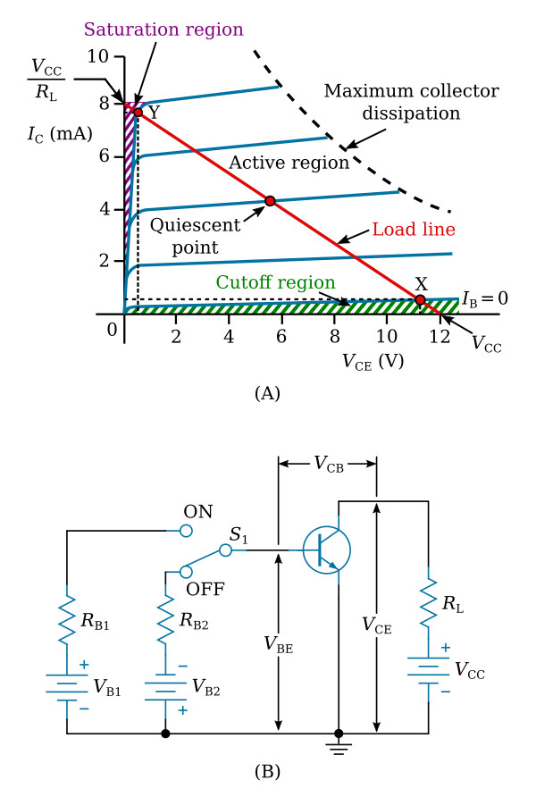
A typical transistor switching circuit is illustrated in part B of the figure above. Switch S1 controls the polarity and amount of base current from battery VB1 or VB2. Resistors RB1 and RB2 are current-limiting resistors. Each region of operation is discussed below.
Cutoff Region
The cutoff region includes the area below the zero base current curve (IB = 0). Ideally, with no initial base current, there would be zero collector current; the collector potential would equal battery voltage VCC. However, at point X on the loadline (view A of the figure above), a small amount of collector current is measured. This is the reverse bias collector current for the common emitter configuration. The collector voltage VCE is indicated by the vertical projection from point X to the collector voltage axis. This value is equal to the difference in magnitude between the battery voltage (12 volts in this instance) and the voltage drop produced by reverse bias collector current flow through load resistor RL. Normal quiescent conditions for a transistor switch in this region require that both emitter-base junction and collector-base junction must be reverse biased.
With switch S1 (see view B of the figure above) in the OFF position, the emitter-base junction is reverse biased by battery VB2 through resistor RB2. The collector-base junction is reverse biased by battery VCC through load resistor RL; the transistor is in the off (cutoff) state. The circuit, as a switch, is open.
Active Region
The active linear region is the only region providing normal amplifier gain. In the linear region, the collector-base junction is reverse biased and the emitter-base junction is forward biased. Transient response of the output signal is essentially determined by transistor characteristics in this region. In switching circuits, this region represents the transition region.
Operation of switch S1 (view B of the figure above) to the ON position establishes the forward bias by battery VB1, through resistor RB1, on the emitter-base junction. The base current IB and collector current IC become transitory in nature, moving from point X on the loadline to point Y; here, collector current reaches saturation. The signal passes through this region rapidly. In switching circuits, this region is of importance only for design considerations.
Saturation Region
In the saturation region (view A of the figure above), an increase in base current does not cause an appreciable increase in collector current IC. At point Y, on the loadline, the transistor is in the saturation region. Collector current IC (measured by a horizontal projection from point Y) is at a maximum, and collector voltage VCE (measured by a vertical projection from point Y) is at a minimum. This value of collector voltage is referred to as the saturation voltage (VCE(SAT)), and is an important characteristic of the transistor. It is usually a fraction of a volt. Deep saturation is generally avoided because of its effect on the transient response of the transistor.
Operating point Y corresponds to a closed switch. Ideally the resistance and voltage from collector to emitter would be zero. In order that a low resistance can be achieved, it is necessary that point Y lie below the knee of the characteristic curves (in the saturation region). Enough base current must be supplied to ensure that this point is reached. It is also important that both the on and off operating points lie in the region below the maximum rated dissipation to avoid transistor destruction.
In calculating the IB necessary to reach point Y, it is necessary to know the current gain (hFE). Knowing hFE gives IBmin since IBmin = IC/hFE. Generally IB is made two or three times greater than IBmin to allow for variations in hFE with temperature.
The maximum rated collector voltage should never be exceeded since destructive heating may occur once a transistor breaks down. Inductive loads can generate injurious voltage transients. These can be avoided by connecting a diode across the inductance to absorb the transient.
Transient Response Characteristics
When switch S1 (view B in the figure above) is operated in sequence from OFF to ON and then back to OFF, the resultant input current pulse IB is similar to that shown in view A of the figure below. The circuit is then characterized by large-signal, or nonlinear, operation of the transistor. In large-signal operation, rectangular input signal drives the transistor from cutoff to saturation and back to cutoff. The distorted output current pulse IC (view B of the figure below) results because the transistor cannot respond instantaneously to a change in signal level. The response of the transistor during rise and fall time is called the transient response of the circuit. The output pulse characteristics are governed primarily by the AC characteristics of the transistor.
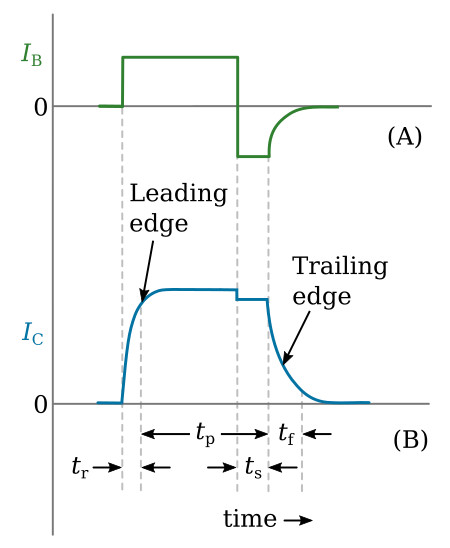
The rise time (tr), also referred to as buildup time or turn-on time, is time required for the leading edge of the pulse to increase in amplitude from 10 to 90 percent of its maximum value. Nonlinear characteristics of the transistor, the external circuit, and energy storage effects contribute to the time. Carriers moving from emitter to collector suffer collision and dispersion and do not reach the collector at the same time. Overdriving the transistor results in decreased rise time. However, the overdrive is normally held to a small value, since the turnoff time (storage time plus fall time, see below), is affected.
The pulse time (tp) or duration time, is the length of time, that the pulse remains at, or near, its maximum value. The pulse time duration is measured from the point on the leading edge where the amplitude of the pulse has reached 90 percent of its maximum value to the point on the trailing edge where the amplitude has fallen to 90 percent of its maximum value.
When the input current, IB, is cut off, the output current, IC, does not immediately fall to zero, but remains almost at its maximum value for a length of time before falling to zero. This period is called the storage time (ts), or saturation delay time. Storage time results from injected minority carriers being in the base region of the transistor at the moment when the input current is cut off. These carriers require a definite length of time to be collected. The length of storage time is essentially governed by the degree of saturation into which the transistor is driven and the time spent in saturation. For high speed switching, storage time is an undesirable condition. Minority carrier storage may be avoided by switching a transistor from its off state to a point in the active region. Collector clamping prevents operation of the transistor in the saturation region.
In the fall time (decay time) tf of the pulse, the amplitude falls from 90 to 10 percent of its maximum value. The fall time of the pulse is essentially determined by the same factors which determine its rise time. Fall time may be slightly reduced through the application of a reverse current at the end of the input pulse.


