


Home > Textbooks > Basic Electronics > Field-Effect Transistors > Junction Field-Effect Transistors >
Field-Effect Transistors
Junction Field-Effect Transistors
Although it has brought about a revolution in the design of electronic equipment, the bipolar (PNP/NPN) transistor still has one very undesirable characteristic. The low input impedance associated with its base-emitter junction causes problems in matching impedances between interstage amplifiers.
For years, scientists searched for a solution that would combine the high input impedance of the vacuum tube with the many other advantages of the transistor. The result of this research is the field-effect transistor (FET). In contrast to the bipolar transistor, which uses bias current between base and emitter to control conductivity, the FET uses voltage to control an electrostatic field within the transistor.
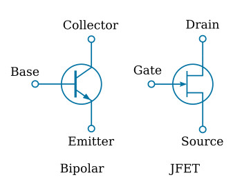
The elements of one type of FET, the junction field-effect transistor (JFET), are compared with the bipolar transistor in the figure below. As the figure shows, the JFET is a three-element device comparable to the other one. The "gate" element of the JFET corresponds very closely in operation to the base of the bipolar transistor. The "source" and "drain" elements of the JFET correspond to the emitter and collector of the bipolar transistor.
JFET Structure
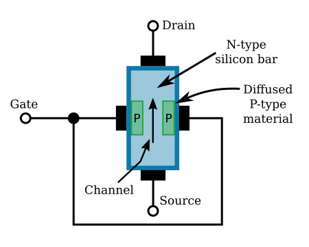
The construction of a JFET is shown in the figure below. A solid bar, made either of N-type or P-type material, forms the main body of the device. Diffused into each side of this bar are two deposits of material of the opposite type from the bar material, which form the "gate." The portion of the bar between the deposits of gate material is of a smaller cross section than the rest of the bar and forms a "channel" connecting the source and the drain. The figure below shows a bar of N-type material and a gate of P-type material. Because the material in the channel is N-type, the device is called an N-channel JFET. In a P-channel JFET, the channel is made of P-type material and the gate of N-type material.
JFET Symbols
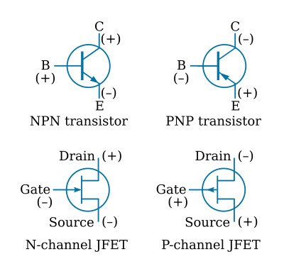
In the figure below, schematic symbols for the two types of JFET are compared with those of the NPN and PNP bipolar transistor. Like the bipolar transistor types, the two types of JFET differ only in the configuration of bias voltages required and in the direction of the arrow within the symbol. Just as it does in bipolar transistor symbols, the arrow in a JFET symbol always points towards the N-type material. Thus the symbol of the N-channel JFET shows the arrow pointing toward the drain/source channel, whereas the P-channel symbol shows the arrow pointing away from the drain/source channel toward the gate.
JFET Biasing
The key to FET operation is the effective cross-sectional area of the channel, which can be controlled by variations in the voltage applied to the gate. This is demonstrated in the figures which follow.
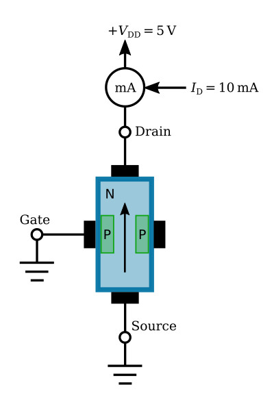
The figure below shows how the JFET operates in a zero gate bias condition. Five volts are applied across the JFET so that electron current flows through the bar from source to drain, as indicated by the arrow. The gate terminal is tied to ground. This is a zero gate bias condition. In this condition, a typical bar represents a resistance of about 500 ohms. A milliammeter, connected in series with the drain lead and DC power, indicates the amount of current flow. With a drain supply (VDD) of 5 volts, the milliammeter gives a drain current (ID) reading of 10 milliamperes. The voltage and current subscript letters (VDD, ID) used for an FET correspond to the elements of the FET just as they do for the elements of transistors.
In the figure below, a small reverse-bias voltage is applied to the gate of the JFET. A gate-source voltage (VGG) of negative 1 volt applied to the P-type gate material causes the junction between the P- and N-type material to become reverse biased. Just as it did in the varactor diode, a reverse-bias condition causes a "depletion region" to form around the PN junction of the JFET. Because this region has a reduced number of current carriers, the effect of reverse biasing is to reduce the effective cross-sectional area of the "channel". This reduction in area increases the source-to-drain resistance of the device and decreases current flow.
The application of a large enough negative voltage to the gate will cause the depletion region to become so large that conduction of current through the bar stops altogether. The voltage required to reduce drain current (ID) to zero is called pinch-off voltage (or threshold voltage) and is comparable to cut-off voltage in a vacuum tube. In the figure above, the negative 1 volt applied, although not large enough to completely stop conduction, has caused the drain current to decrease markedly (from 10 milliamperes under zero gate bias conditions to 5 milliamperes). Calculation shows that the 1-volt gate bias has also increased the resistance of the JFET (from 500 ohms to 1 kilohm). In other words, a 1-volt change in gate voltage has doubled the resistance of the device and cut current flow in half.
These measurements, however, show only that a JFET operates in a manner similar to a bipolar transistor, even though the two are constructed differently. As stated before, the main advantage of an FET is that its input impedance is significantly higher than that of a bipolar transistor. The higher input impedance of the JFET under reverse gate bias conditions can be seen by connecting a microammeter in series with the gate-source voltage (VGG), as shown in the figure below.
With a VGG of 1 volt, the microammeter reads 0.5 microamps. Applying Ohm's law (1 V / 0.5 µA) illustrates that this very small amount of current flow results in a very high input impedance (about 2 megaohms). By contrast, a bipolar transistor in similar circumstances would require higher current flow (e.g., 0.1 to 1 mA), resulting in a much lower input impedance (about 1000 ohms or less). The higher input impedance of the JFET is possible because of the way reverse-bias gate voltage affects the cross-sectional area of the channel.
The preceding example of JFET operation uses an N-channel JFET. However, a P-channel JFET operates on identical principles. The differences between the two types are shown in the figure below.
Because the materials used to make the bar and the gate are reversed, source voltage potentials must also be reversed. The P-channel JFET therefore requires a positive gate voltage to be reverse biased, and electron current flows through it from drain to source.
Output characteristic curves of JFET
A plot (figure below) of drain (output) current ID vs. drain-source voltage VDS, with gain-source voltage VGS as parameter shows two regions: the ohmic region in which the JFET acts as a resistor of variable resistance depending on the gate voltage, and a saturation region in which drain current is almost unaffected by drain-source voltage (constant-current region). Note that when the drain-source voltage becomes too large there is a sudden rise of current, indicating ionization breakdown of the semiconductor crystal.
Operating characteristics of JFET
The three most important operating characteristics of the device are:
- Pinch-off voltage VP
- Drain current IDSS in pinch-off (saturation) region at zero-gate bias (VGS = 0)
- Transconductance gm
The pinch-off voltage is the value of gate-to-source bias voltage (for zero or small drain-source voltage), for which the depletion region penetrates (from both sides) the entire thickness of the channel thus "pinching off" the current flow. With a zero gate-to-source bias voltage the current flow is a maximum.
Several transfer characteristics (ID-VGS) using various simplifying approximations have been derived. The most useful may be adapted from Richer and Middlebrook [1], who stated that the drain current in the pinch-off (saturation) region is

For many JFET devices, n is very close to 2.
JFETs provide a gain measured in terms of transconductance, gm. Transconductance in the pinch-off (saturation) region is given by

If n = 2, transconductance is a linear function of input voltage (VGS).
JFET amplifier
The figure below shows a basic common-source amplifier circuit containing an N-channel JFET. The characteristics of this circuit include high input impedance and a high voltage gain. The function of the circuit components in this figure is very similar to those in a bipolar junction transistor common-emitter amplifier circuit. C1 and C3 are the input and output coupling capacitors. R1 is the gate return resistor. It prevents unwanted charge buildup on the gate by providing a discharge path for C1. R2 and C2 provide source self-bias for the JFET, which operates like emitter self-bias. R3 is the drain load resistor, which acts like the collector load resistor.
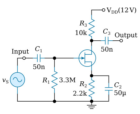
The phase shift of 180 degrees between input and output signals is the same as that of common-emitter transistor circuits. The reason for the phase shift can be seen easily by observing the operation of the N-channel JFET. On the positive alternation of the input signal, the amount of reverse bias on the P-type gate material is reduced, thus increasing the effective cross-sectional area of the channel and decreasing source-to-drain resistance. When resistance decreases, current flow through the JFET increases. This increase causes the voltage drop across R3 to increase, which in turn causes the drain voltage to decrease. On the negative alternation of the cycle, the amount of reverse bias on the gate of the JFET is increased and the action of the circuit is reversed. The result is an output signal, which is an amplified 180-degree-out-of-phase version of the input signal.
References:
- Richer, I., and Middlebrook, R. D., "Power Law Nature of Field-Effect Transistor Experimental Characteristics," Proceedings, IEEE, Vol. 51, pp. 1145—1146, August 1963.


