


Home > Textbooks > Basic Electronics > Audio Amplifiers > Volume Controls >
Audio Amplifiers
Volume Controls
The current, voltage, and power gains of transistor stages are usually varied by using variable resistors in the coupling networks. The variable resistor is usually referred to as a gain control. At audio frequencies, the gain control is referred to as a volume control.
The volume control and its associated circuit should permit the variation of gain from zero to maximum. Moreover, the volume control should be so arranged in a given circuit that all frequencies are attenuated equally for all positions of the variable arm of the control.
A large number of satisfactory volume control circuits can be designed. A typical volume control circuit is discussed below.
The two-stage amplifier (see the figure below) uses variable resistor R2 as a volume control. Collector load resistor R1 develops transistor Q1 output signal. DC blocking capacitor C1 couples the signal to variable resistor R2 and the transistor Q2 input circuit. Resistors R4 and R3 form a voltage divider to establish the base bias voltage. Resistor R5 is the emitter swamping resistor and is AC bypassed by capacitor C2. Collector load resistor R6 develops the output signal. Placement of variable resistor R2 in the circuit as shown is unsatisfactory for the reasons stated below.
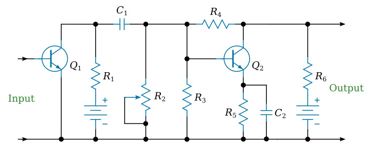
(1) The base bias voltage is that voltage developed across resistor R3. This voltage will vary from a maximum to zero depending on the position of the variable arm on variable resistor R2. The voltage developed across resistor R3 must cancel the opposing voltage developed across swamping resistor R5 and leave a net forward base-emitter bias. This condition will not be met with variable resistor R2 shunting resistor R3.
(2) The DC current flowing through variable resistor R2 will cause excessive noise.
(3) The gain of the low frequencies will vary according to the position of the variable arm on variable resistor R2. This condition can be understood by considering the base-emitter junction resistance of transistor Q2 as negligibly small. With this assumption, variable resistor R2 can be considered as shunting emitter swamping resistor R5. With all of the resistance of variable resistor R2 in the circuit, capacitor C2 effectively bypasses the low frequencies around the parallel combination of resistor R5 and variable resistor R2 to minimize degeneration of the low frequencies. As the variable arm moves to reduce the portion of variable resistor R2 in the circuit, capacitor C2 becomes less effective as a bypass capacitor for the low frequencies, causing greater degeneration of the low frequencies compared to the high frequencies.
The circuit shown in the figure below avoids the unsatisfactory conditions found in the circuit shown in the figure above. The functions of the parts of the two circuits bearing the same reference symbols are the same. DC blocking capacitor C3 has been added to the circuit of the figure below.
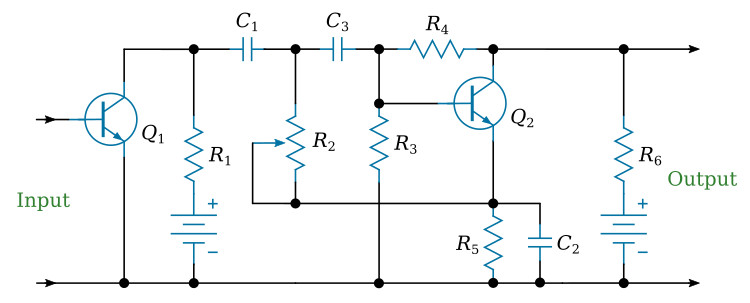
Capacitor C3 avoids the variation in base bias voltage by DC isolating resistor R2 from resistor R3. The noise factor of the amplifier is also improved by preventing DC current flow through the variable resistor.
By connecting the lower end of variable resistor R2 to the upper end of resistor R5 and capacitor C2, variable resistor R2 does not AC shunt resistor R5 and capacitor C2. This arrangement avoids the deterioration of the low-frequency response of the amplifier as the resistance of variable resistor R2 is reduced.


