Home > Textbooks > Basic Electronics > Diodes > Tunnel Diodes >
Diodes
Tunnel Diodes
In 1957, Leo Esaki, a Japanese scientist, discovered that if a semiconductor junction diode is heavily doped with impurities, it will have a region of negative resistance. The normal junction diode uses semiconductor materials that are lightly doped with one impurity atom for ten-million semiconductor atoms. This low doping level results in a relatively wide depletion region. Conduction occurs in the normal junction diode only if the voltage applied to it is large enough to overcome the potential barrier of the junction.
In the tunnel diode, the semiconductor materials used in forming a junction are doped to the extent of one-thousand impurity atoms for ten-million semiconductor atoms. This heavy doping produces an extremely narrow depletion zone similar to that in the Zener diode. Also because of the heavy doping, a tunnel diode exhibits an unusual current-voltage characteristic curve as compared with that of an ordinary junction diode. The characteristic curve for a tunnel diode is illustrated in the figure below.
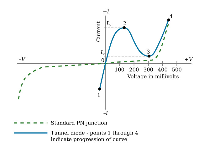
The three most important aspects of this characteristic curve are (1) the forward current increase to a peak (Ip) with a small applied forward bias, (2) the decreasing forward current with an increasing forward bias to a minimum valley current (Iv), and (3) the normal increasing forward current with further increases in the bias voltage. The portion of the characteristic curve between Ip and Iv is the region of negative resistance. An explanation of why a tunnel diode has a region of negative resistance is best understood by using energy levels as in the previous explanation of the Zener effect.
Simply stated the theory known as quantum-mechanical tunneling is an electron crossing a PN-junction without having sufficient energy to do so otherwise. Because of the heavy doping the width of the depletion region is only one-millionth of an inch. You might think of the process simply as an arc-over between the N- and the P-side across the depletion region.
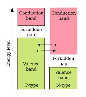
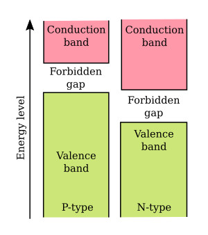
The figure below shows the energy level diagram of a tunnel diode with no bias applied. Note that there is an overlap of the two energy bands. The valence band of the P-material overlaps the conduction band of the N-material. In the overlapped region, an electron can move from the valence band in the P-material to the conduction band in the N-material, or vice versa, without a change in its energy, because parts of the two bands are on the same level. When empty energy states exist in the overlapped region, the internal field is great enough (without bias) for some electrons to change bands without a change in energy. This movement of electrons across the junction without a change in energy is known as tunneling. In the unbiased diode the net current is zero so that the tunneling current of electrons moving from the conduction band to the valence band is equal to the tunneling current of electrons moving from the valence to the conduction band. The zero net current flow is marked by an "0" on the current-voltage curve illustrated in the top figure.
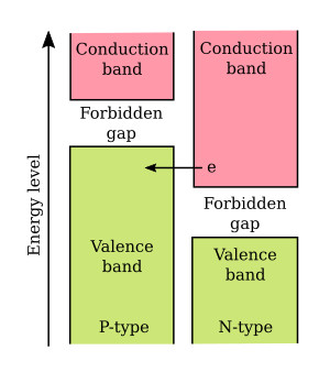
The figure below shows the energy diagram of a tunnel diode with a small forward bias (50 millivolts) applied. The bias causes unequal energy levels between some of the majority carriers at the energy band overlap point. Note that the amount of overlap between the valence band of the P-material and the conduction band of the N-material decreased. Since the valence band and the conduction band still overlap, current carriers tunnel across at the overlap and cause a substantial current flow.
As the forward bias is further increased, the current will increase until it will reach a peak value (Ip). This amount of current flow is marked by point 2 on the current-voltage curve in the top figure. The portion of the current-voltage curve from point 2 to point 3 shows the decreasing current that occurs as the bias is increased, and the area of overlap becomes smaller. As the overlap between the two energy bands becomes smaller, fewer and fewer electrons can tunnel across the junction. The portion of the curve between point 2 and point 3 in which current decreases as the voltage increases is the negative resistance region of the tunnel diode.
The figure below is the energy diagram of a tunnel diode in which the forward bias has been increased to 450 millivolts. As you can see, the valence band and the conduction band no longer overlap at this point, and tunneling can no longer occur. The tunnel diode starts to operate in the same manner as a normal PN junction, as shown by the portion of the current-voltage curve in the top figure from point 3 to point 4.
The negative resistance region is the most important and most widely used characteristic of the tunnel diode. A tunnel diode biased to operate in the negative resistance region can be used as either an oscillator or an amplifier in a wide range of frequencies and applications. Very high frequency applications using the tunnel diode are possible because the tunneling action occurs so rapidly that there is no transit time effect and therefore no signal distortion. Tunnel diodes are also used extensively in high-speed switching circuits because of the speed of the tunneling action.
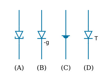
Several schematic symbols are used to indicate tunnel diode. These symbols are illustrated in views A through D of the figure below.