Home > Textbooks > Basic Electronics > Diodes > Semiconductor Theory >
Diodes
Semiconductor Theory
Two of the most widely known semiconductors in use today are the junction diode and transistor. These semiconductors fall under a more general heading called solid-state devices. A solid-state device is nothing more than an electronic device, which operates by virtue of the movement of electrons within a solid piece of semiconductor material.
Since the invention of the transistor, solid-state devices have been developed and improved at an unbelievable rate. Great strides have been made in the manufacturing techniques, and there is no foreseeable limit to the future of these devices. Solid-state devices made from semiconductor materials offer compactness, efficiency, ruggedness, and versatility. Consequently, these devices have invaded virtually every field of science and industry. In addition to the junction diode and transistor, a whole new family of related devices has been developed: the zener diode, light-emitting diode, field effect transistor, etc. One development that has dominated solid-state technology, and probably has had a greater impact on the electronics industry than either the electron tube or transistor, is the integrated circuit. The integrated circuit is a minute piece of semiconductor material that can produce complete electronic circuit functions.
Atomic Structure
Matter is anything that occupies space and has weight. Rocks, water, air, automobiles, clothing, and even our own bodies are good examples of matter. Matter may be found in any one of three states: solids, liquids, and gases. All matter is composed of either an element or combination of elements. Examples of elements are iron, gold, silver, copper, and oxygen.
As we work our way down the size scale, we come to the atom, the smallest particle into which an element can be broken down and still retain all its original properties. The atom is basically composed of electrons, protons, and neutrons. Furthermore, the electrons, protons, and neutrons of one element are identical to those of any other element. There are different kinds of elements because the number and the arrangement of electrons and protons are different for each element.
Energy Bands
The path each electron takes around the nucleus of atom is called an orbit. The orbiting electrons do not follow random paths, instead they are confined to definite energy levels. These levels can be visualized as shells with each successive shell being spaced a greater distance from the nucleus. The outer shell of an atom is called valence shell, and the electrons contained in this shell are called valence electrons.
To move an electron from a lower shell to a higher shell a certain amount of energy is required. This energy can be in the form of electric fields, heat, light, and even bombardment by other particles. Failure to provide enough energy to the electron, even if the energy supplied is just short of the required amount, will cause it to remain at its present energy level. Supplying more energy than is needed will only cause the electron to move to the next higher shell and the remaining energy will be wasted. In simple terms, energy is required in definite units to move electrons from one shell to the next higher shell. These units are called quanta (for example 1, 2, or 3 quanta).
Electrons can also lose energy as well as receive it. When an electron loses energy, it moves to a lower shell. The lost energy, in some cases, appears as heat.
If a sufficient amount of energy is absorbed by an electron, it is possible for that electron to be completely removed from the influence of the atom. This is called ionization. When an atom loses electrons or gains electrons in this process of electron exchange, it is said to be ionized. For ionization to take place, there must be a transfer of energy that results in a change in the internal energy of the atom. An atom having more than its normal amount of electrons acquires a negative charge, and is called a negative ion. The atom that gives up some of its normal electrons is left with fewer negative charges than positive charges and is called a positive ion. Thus, we can define ionization as the process by which an atom loses or gains electrons.
Up to this point in our discussion, we have spoken only of isolated atoms. When atoms are spaced far enough apart, as in a gas, they have very little influence upon each other, and are very much like lone atoms. But atoms within a solid have a marked effect upon each other. The forces that bind these atoms together greatly modify the behavior of the other electrons. One consequence of this close proximity of atoms is to cause the individual energy levels of an atom to break up and form bands of energy. Discrete (separate and complete) energy levels still exist within these energy bands, but there are many more energy levels than there were with the isolated atom. In some cases, energy levels will have disappeared. The figure below shows the difference in the energy arrangement between an isolated atom and the atom in a solid. Notice that the isolated atom (such as in gas) has energy levels, whereas the atom in a solid has energy levels grouped into energy bands.
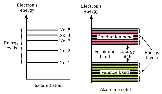
The upper band in the solid lines in the figure above is called the conduction band because electrons in this band are easily removed by the application of external electric fields. Materials that have a large number of electrons in the conduction band act as good conductors of electricity.
Below the conduction band is the forbidden band or energy gap. Electrons are never found in this band, but may travel back and forth through it, provided they do not come to rest in the band.
The last band or valence band is composed of a series of energy levels containing valence electrons. Electrons in this band are more tightly bound to the individual atom than the electrons in the conduction band. However, the electrons in the valence band can still be moved to the conduction band with the application of energy, usually thermal energy. There are more bands below the valence band, but they are not important to the understanding of semiconductor theory and will not be discussed.
The concept of energy bands is particularly important in classifying materials as conductors, semiconductors, and insulators. An electron can exist in either of two energy bands, the conduction band or the valence band. All that is necessary to move an electron from the valence band to the conduction band so it can be used for electric current, is enough energy to carry the electron through the forbidden band. The width of the forbidden band or the separation between the conduction and valence bands determines whether a substance is an insulator, semiconductor, or conductor. The figure below uses energy level diagrams to show the difference between insulators, semiconductors, and conductors.
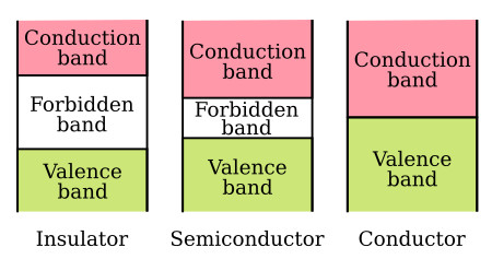
The energy diagram for the insulator shows the insulator with a very wide energy gap. The wider this gap, the greater the amount of energy required to move the electron from the valence band to the conduction band. Therefore, an insulator requires a large amount of energy to obtain a small amount of current. The insulator "insulates" because of the wide forbidden band or energy gap.
The semiconductor, on the other hand, has a smaller forbidden band and requires less energy to move an electron from the valence band to the conduction band. Therefore, for a certain amount of applied voltage, more current will flow in the semiconductor than in the insulator.
The last energy level diagram in the figure above is that of a conductor. Notice, there is no forbidden band or energy gap and the valence and conduction bands overlap. With no energy gap, it takes a small amount of energy to move electrons into the conduction band; consequently, conductors pass electrons very easily.
Covalent Bonding
The chemical activity of an atom is determined by the number of electrons in its valence shell. When the valence shell is complete, the atom is stable and shows little tendency to combine with other atoms to form solids. Only atoms that possess eight valence electrons have a complete outer shell. These atoms are referred to as inert or inactive atoms. However, if the valence shell of an atom lacks the required number of electrons to complete the shell, then the activity of the atom increases.
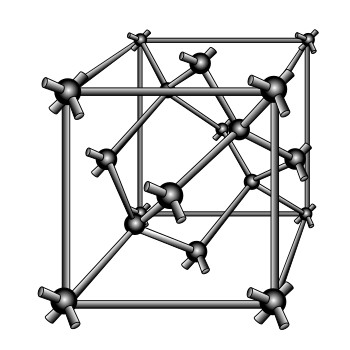
Silicon and germanium, for example, are frequently used semiconductors. Both are quite similar in their structure and chemical behavior. Each has four electrons in the valence shell. Consider just silicon. Since it has fewer than the required number of eight electrons needed in the outer shell, its atoms will unite with other atoms until eight electrons are shared. This gives each atom a total of eight electrons in its valence shell; four of its own and four that it borrowed from the surrounding atoms. The sharing of valence electrons between two or more atoms produces a covalent bond between the atoms. It is this bond that holds the atoms together in an orderly structure called a crystal. A crystal is just another name for a solid whose atoms or molecules are arranged in a three-dimensional geometrical pattern commonly referred to as a lattice. The figure below shows a typical crystal structure. Each sphere in the figure represents the nucleus of an atom, and the arms that join the atoms and support the structure are the covalent bonds.
As a result of this sharing process, the valence electrons are held tightly together. This can best be illustrated by the two-dimensional view of the silicon lattice in the figure below. The circles in the figure represent the nuclei of the atoms. The +4 in the circles is the net charge of the nucleus plus the inner shells (minus the valence shell). The short lines indicate valence electrons. Because every atom in this pattern is bonded to four other atoms, the electrons are not free to move within the crystal. As a result of this bonding, pure silicon and germanium are poor conductors of electricity. The reason they are not insulators but semiconductors is that with the proper application of heat or electrical pressure, electrons can be caused to break free of their bonds and move into the conduction band. Once in this band, they wander aimlessly through the crystal.

Conduction Process
As stated earlier, energy can be added to electrons by applying heat. When enough energy is absorbed by the valence electrons, it is possible for them to break some of their covalent bonds. Once the bonds are broken, the electrons move to the conduction band where they are capable of supporting electric current. When a voltage is applied to a crystal containing these conduction band electrons, the electrons move through the crystal toward the applied voltage. This movement of electrons in a semiconductor is referred to as electron current flow.
There is still another type of current in a pure semiconductor. This current occurs when a covalent bond is broken and a vacancy is left in the atom by the missing valence electron. This vacancy is commonly referred to as a hole. The hole is considered to have a positive charge because its atom is deficient by one electron, which causes the protons to outnumber the electrons. As a result of this hole, a chain reaction begins when a nearby electron breaks its own covalent bond to fill the hole, leaving another hole. Then another electron breaks its bond to fill the previous hole, leaving still another hole. Each time an electron in this process fills a hole, it enters into a covalent bond. Even though an electron has moved from one covalent bond to another, the most important thing to remember is that the hole is also moving. Therefore, since this process of conduction resembles the movement of holes rather than electrons, it is termed hole flow (short for hole current flow or conduction by holes). Hole flow is very similar to electron flow except that the holes move toward a negative potential and in an opposite direction to that of the electron. Since hole flow results from the breaking of covalent bonds, which are at the valence band level, the electrons associated with this type of conduction contain only valence band energy and must remain in the valence band. However, the electrons associated with electron flow have conduction band energy and can, therefore, move throughout the crystal. A good analogy of hole flow is the movement of a hole through a tube filled with balls (see the figure below).
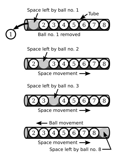
When ball number 1 is removed from the tube, a hole is left. This hole is then filled by ball number 2, which leaves still another hole. Ball number 3 then moves into the hole left by ball number 2. This causes still another hole to appear where ball 3 was. Notice the holes are moving to the right side of the tube. This action continues until all the balls have moved one space to the left in which time the hole moved eight spaces to the right and came to rest at the right-hand end of the tube.
In the theory just described, two current carriers were created by the breaking of covalent bonds: the negative electron and the positive hole. These carriers are referred to as electron-hole pairs. Since the semiconductor we have been discussing contains no impurities, the number of holes in the electron-hole pairs is always equal to the number of conduction electrons. Another way of describing this condition where no impurities exist is by saying the semiconductor is intrinsic. The term intrinsic is also used to distinguish the pure semiconductor that we have been working with from one containing impurities.
Doping Process
The pure semiconductor mentioned earlier is basically neutral. It contains no free electrons in its conduction bands. Even with the application of thermal energy, only a few covalent bonds are broken, yielding a relatively small current flow. A much more efficient method of increasing current flow in semiconductors is by adding very small amounts of selected additives to them, generally no more than a few parts per million. These additives are called impurities and the process of adding them to crystals is referred to as doping. The purpose of semiconductor doping is to increase the number of free charges that can be moved by an external applied voltage. When an impurity increases the number of free electrons, the doped semiconductor is negative or N type, and the impurity that is added is known as an N-type impurity. However, an impurity that reduces the number of free electrons, causing more holes, creates a positive or P-type semiconductor, and the impurity that was added to it is known as a P-type impurity. Semiconductors which are doped in this manner – either with N- or P-type impurities – are referred to as extrinsic semiconductors.
N-Type Semiconductor
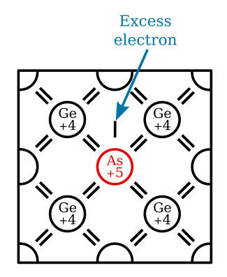
The N-type impurity loses its extra valence electron easily when added to a semiconductor material, and in so doing, increases the conductivity of the material by contributing a free electron. This type of impurity has 5 valence electrons and is called a pentavalent impurity. Arsenic, antimony, bismuth, and phosphorous are pentavalent impurities. Because these materials give or donate one electron to the doped material, they are also called donor impurities.
When a pentavalent (donor) impurity, like arsenic, is added to germanium, it will form covalent bonds with the germanium atoms. The figure below illustrates this by showing an arsenic atom (As) in a germanium (Ge) lattice structure. Notice the arsenic atom in the center of the lattice. It has 5 valence electrons in its outer shell but uses only 4 of them to form covalent bonds with the germanium atoms, leaving 1 electron relatively free in the crystal structure. Pure germanium may be converted into an N-type semiconductor by "doping" it with any donor impurity having 5 valence electrons in its outer shell. Since this type of semiconductor (N-type) has a surplus of electrons, the electrons are considered majority carriers, while the holes, being few in number, are the minority carriers.
P-Type Semiconductor
The second type of impurity, when added to a semiconductor material, tends to compensate for its deficiency of 1 valence electron by acquiring an electron from its neighbor. Impurities of this type have only 3 valence electrons and are called trivalent impurities. Aluminum, indium, gallium, and boron are trivalent impurities. Because these materials accept 1 electron from the doped material, they are also called acceptor impurities.
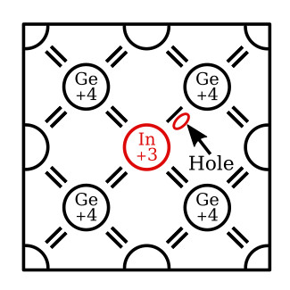
A trivalent (acceptor) impurity element can also be used to dope germanium. In this case, the impurity is 1 electron short of the required amount of electrons needed to establish covalent bonds with 4 neighboring atoms. Thus, in a single covalent bond, there will be only 1 electron instead of 2. This arrangement leaves a hole in that covalent bond. The figure below illustrates this theory by showing what happens when germanium is doped with an indium (In) atom. Notice, the indium atom in the figure is 1 electron short of the required amount of electrons needed to form covalent bonds with 4 neighboring atoms and, therefore, creates a hole in the structure. Gallium and boron, which are also trivalent impurities, exhibit these same characteristics when added to germanium. The holes can only be present in this type semiconductor when a trivalent impurity is used. Note that a hole carrier is not created by the removal of an electron from a neutral atom, but is created when a trivalent impurity enters into covalent bonds with a tetravalent (4 valence electrons) crystal structure. The holes in this type of semiconductor (P-type) are considered the majority carriers since they are present in the material in the greatest quantity. The electrons, on the other hand, are the minority carriers.