


Home > Textbooks > Basic Electronics > Power Sources > Switched-Mode Power Supply >
Power Sources
Switched-Mode Power Supply
Switched-mode power supplies have distinct advantage over linear power supplies: low power dissipation in the main control device (switching regulator).
The switching regulator can achieve efficiencies approaching 100 percent. Such a regulator utilizes a semiconductor (e.g. transistor) which is rapidly switched between its limiting conducting and non-conducting states. Regulation control is obtained by varying the conducting time (duty cycle) during each cycle of switching. Semiconductor switches can be made to have very small dissipation of power in both the conducting and non-conducting states. The only appreciable dissipation of power occurs during the transitions between states, and this is minimized by rapid switching using a suitable switching frequency. The bursts of power passed by the semiconductor must be filtered to produce usable DC power. The net result is a high efficiency and good voltage regulation. The following paragraphs discuss the basic types of switching regulators.
Buck Regulator
One of the first switching type DC regulator circuits used the same series transistor as the simple linear series regulator, but turned it full on or full off depending on how the output voltage compared with a reference. A simple LC filter smoothed out the large voltage variations caused by this switching, and a flyback diode was added to provide a path for the inductor current during the periods when the series switch was off. The resulting circuit is shown in the figure below.
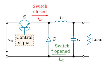
The output voltage is related to the input voltage by the ratio ton/T, where ton is the ON time of the switch and T is the period of control signal.
Because of the inductor, this type of regulator is usually heavier (for a given current) than the linear regulator (series or shunt), but this difference can be minimized by performing the switching at as high a frequency as possible (consistent with transistor switching losses) to reduce the inductor size. Since this is a switching type regulator, it is also possible to use SCRs in place of the transistor. With SCRs the circuits become more complex, because of the necessity of having some method for turning the SCR off. Both the transistor and SCR buck type switching regulators provide an output voltage which can be no greater than the input.
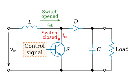
Boost Regulator
The boost (step-up) circuit shown in the figure below provides an output not less than the input voltage. It operates in the following manner. When the switch S (shown as a transistor in the figure below) is turned on, current from the source builds up in L (and S). The inductor L stores energy during this time. When S is opened, a voltage is induced in the inductor. This voltage adds to the voltage of the input source vin and the inductor discharges through D into C, charging it. The current in L decays until the switch turns on again. While the switch is closed and current is building up in L, the load current is supplied entirely by capacitor C.
The ratio of output to input voltage is T to toff, with T the period of control signal and toff the OFF time of the switching element.
Buck-Boost Regulator
The buck-boost regulator is shown in the figure below. The energy-storage inductor L stores energy during on-time interval when switch (transistor) S is conducting. In this time, the load current is supplied by capacitor C. When the switch is turned off, a voltage with the polarity opposite to that of the input voltage is induced in the inductor and the energy previously stored in the inductor is delivered to the capacitor and load.
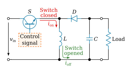
The output voltage is related to input voltage by the ratio ton/toff, which are, respectively, the ON and OFF times of the switch.


