


Home > Textbooks > Selected Circuits > Power Supplies > Transistor Current Regulator >
Power Supplies
Transistor Current Regulator
A schematic diagram of the current regulator is shown below. The nominal input voltage to this regulator is 14.5 volts. Variations in input voltage from about 12 to 16 volts can be tolerated. Easy and accurate adjustment of the output current (through the load RL) in the range of 10 to 100 mA is provided by means of a precision potentiometer (R5).
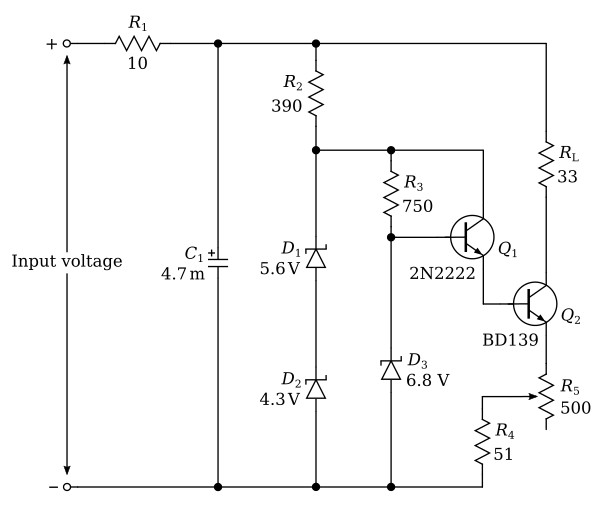
The filtering circuit at the input consists of a single-section RC filter (R1 and C1) with a time constant of 0.047 s and a DC impedance of 10 Ω. A stable reference voltage is established across the 6.8-volt Zener diode (D3). Variations in this reference voltage due to input voltage variations are greatly reduced through preregulation using two series Zener diodes (D1 and D2) operating at about 9.9 volts. These two diodes are also used to stabilize the collector voltage of the first amplifying transistor Q1, and hence improve the gain stability of this emitter-follower stage.
The output load of the first transistor (Q1) is the input base of the current-regulating transistor (Q2). The high current gain of the dual, direct-coupled, emitter-follower configuration provides extremely stable emitter voltage at the regulating transistor (Q1) with a very small current input from the reference diode (D3). Since the current change from the reference diode is small for wide variations in output current, the regulating effects are almost linear with the value of emitter resistance. A DC potential change of 1.4 volts normally occurs across the two transistor junctions so that the emitter of the regulating transistor is held at about +5.4 volts with respect to the negative input lead. The current through the emitter resistors (R4 and R5) is then equal to 5.4 volts divided by the resistance value and, hence, remains as constant as the reference voltage across D3. The output current at the collector of the transistor is then

where
IC is the collector output current,
β is the transistor current gain, and
IE is the emitter current.
As this equation shows, if β is greater than about 20, large changes in β cause only small changes in the output current. The β of the regulating transistor can be expected to vary with changes in collector-to-emitter voltage and transistor junction temperature.
