Home > Textbooks > Basic Electronics > Wave Shaping > Positive Diode Clampers >
Wave Shaping
Positive Diode Clampers
The figure below, view A, illustrates the circuit of a positive diode clamper. Resistor R1 provides a discharge path for C1. This resistance is large in value so that the discharge time of C1 will be long compared to the input pulse width. The diode provides a fast charge path for C1. After C1 becomes charged it acts as a voltage source. The input wave shape shown in view B is a square wave and varies between +25 volts and -25 volts. Compare each portion of the input wave shape with the corresponding output wave shape. Keep Kirchhoff's law in mind: The algebraic sum of the voltage drops around a closed loop is 0 at any instant.
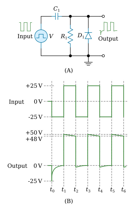
At t0 the -25 volt input signal appears across R1 and D1 (the capacitor is a short at the first instant). The initial voltage across R1 and D1 causes a voltage spike in the output. Because the charge time of C1 through D1 is almost instantaneous, the duration of the pulse is so short that it has only a negligible effect on the output. The -25 volts across D1 makes the cathode negative with respect to the anode and the diode conducts heavily. C1 quickly charges through the small resistance of D1. As the voltage across C1 increases, the output voltage decreases at the same rate. The voltage across C1 reaches -25 volts and the output is at 0 volts.
At t1 the +25 volts already across the capacitor and the +25 volts from the input signal are in series and aid each other (series aiding). Thus, +50 volts appears across R1 and D1. At this time, the cathode of D1 is positive with respect to the anode, and the diode does not conduct. From t1 to t2, C1 discharges to approximately +23 volts (because of the large values of R1 and C1) and the output voltage drops from +50 volts to +48 volts.
At t2 the input signal changes from +25 volts to -25 volts. The input is now series opposing with the +23 volts across C1. This leaves an output voltage of -2 volts (-25 plus +23 volts). The cathode of D1 is negative with respect to the anode and D1 conducts. From t2 to t3, C1 quickly charges through D1 from +23 volts to +25 volts; the output voltage changes from -2 volts to 0 volts.
At t3 the input signal and capacitor voltage are again series aiding. Thus, the output voltage felt across R1 and D1 is again +50 volts. During t3 and t4, C1 discharges 2 volts through R1. Notice that circuit operation from t3 to t4 is the same as it was from t1 to t2. The circuit operation for each square-wave cycle repeats the operation which occurred from t2 to t4.
Compare the input wave shape of the figure above, view B, with the output wave shape. Note the following important points: (1) The peak-to-peak amplitude of the input wave shape has not been changed by the clamper circuit; (2) the shape of the output wave shape has not been significantly changed from that of the input by the action of the clamper circuit; and (3) the output wave shape is now all above 0 volts whereas the input wave shape is both above and below 0 volts. Thus, the lower part of the input wave shape has been clamped to a DC potential of 0 volts in the output. This circuit is referred to as a positive clamper since all of the output wave shape is above 0 volts and the bottom is clamped at 0 volts.
The positive clamper circuit is self-adjusting. This means that the bottom of the output waveform remains clamped at 0 volts during changes in input signal amplitude. Also, the output wave shape retains the form and peak-to-peak amplitude (50 volts in this case) of the input wave shape. When the input amplitude becomes greater, the charge of the capacitor becomes greater and the output amplitude becomes larger. When the input amplitude decreases, the capacitor does not charge as high as before and clamping occurs at a lower output voltage. The capacitor charge, therefore, changes with signal strength.
The size of R1 and C1 has a direct effect upon the operation of the clamper. Because of the small resistance of the diode, the capacitor charge time is short. If either R1 or C1 is made smaller, the capacitor discharges faster (tC = R × C).
The ability of a smaller value capacitor to quickly discharge to a lower voltage is an advantage when the amplitude of the input wave shape is suddenly reduced. However, for normal clamper operation, quick discharge time is a disadvantage. This is because one objective of clamping is to keep the output wave shape the same as the input wave shape. If the small capacitor allows a relatively large amount of the voltage to discharge with each cycle, then distortion occurs in the output wave shape. A larger portion of the wave shape then appears on the wrong side of the reference line.
Increasing the value of the resistor increases the discharge time (again, tC = R × C). This increased value causes the capacitor to discharge more slowly and produces an output wave shape which is a better reproduction of the input wave shape. A disadvantage of increasing the resistance value is that the larger resistance increases the discharge time of the capacitor and slows the self-adjustment rate of the circuit, particularly in case a sudden decrease in input amplitude should occur. The larger resistance has no effect on self-adjustment with a sudden rise in input amplitude. This is because the capacitor charges through the small resistance of the conducting diode. Circuits often incorporate a compromise between a short RC time constant (for self-adjustment purposes) and a long RC time constant for less distortion.
Positive Diode Clampers With Bias
Biased clamping circuits operate in exactly the same manner as unbiased clampers, with one exception. That exception is the addition of a DC bias voltage in series with the diode and resistor. The size and polarity of this bias voltage determines the output clamping reference.
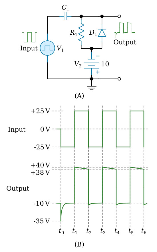
View A of the figure below illustrates the circuit of a positive clamper with positive bias. It can be identified as a positive clamper because the cathode of the diode is connected to the capacitor. Positive bias can be observed by noting that the negative side of the battery is connected to ground. The purposes and actions of the capacitor, resistor, and diode are the same as in the unbiased clamper circuit just discussed.
With no input, D1 is forward biased and the +10 V battery is the output. C1 will charge to +10 V and hold this charge until the first pulse is applied. The battery establishes the DC reference level at +10 volts. The input wave shape at the top of view B is a square wave which alternates between +25 and -25 volts. The output wave shape is shown at the bottom half of view B.
Here, as with previous circuits, let's apply Kirchhoff's voltage law to determine circuit operation. With no input signal, the output is just the +10 volts supplied by the battery.
At time t0 the -25 volt signal applied to the circuit is instantly felt across R1 and D1. The -25 volt input signal forward biases D1, and C1 quickly charges to 35 volts. This leaves +10 volts across the output terminals for much of the period from t0 to t1. The polarity of the charged capacitor is, from the left to the right, minus to plus.
At t1 the 35 volts across the capacitor is series aiding with the +25 volt input signal. At this point (t1) the output voltage becomes +60 volts; the voltage across R1 and D1 is +50 volts, and the battery is +10 volts. The cathode of D1 is positive with respect to the anode and the diode does not conduct. From t1 to t2, C1 discharges only slightly through the large resistance of R1. Assume that, because of the size of R1 and C1, the capacitor discharges just 2 volts (from +35 volts to +33 volts) during this period. Thus, the output voltage drops from +60 volts to +58 volts.
At t2 the -25 volt input signal and the +33 volts across C1 are series opposing. This makes the voltage across the output terminals +8 volts. The cathode of the diode is 2 volts negative with respect to its anode and D1 conducts. Again, since the forward-biased diode is essentially a short, C1 quickly charges from +33 volts to +35 volts. During most of the time from t2 to t3, then, we find the output voltage is +10 volts.
At t3 the +25 volts of the input signal is series aiding with the +35 volts across C1. Again the output voltage is +60 volts. Observe that at t3 the conditions in the circuit are the same as they were at t1. Therefore, the circuit operation from t3 to t4 is the same as it was from t1 to t2. Circuit operation continues as a duplication of the operations which occurred from t1 to t3.
By comparing the input and output wave shapes, you should note the following: (1) The peak-to-peak amplitude of the input wave shape has not been changed in the output (for all practical purposes) by the action of the clamper circuit; (2) the shape of the input wave has not been changed; (3) the output wave shape is now clamped above +10 volts. Remember that this clamping level (+10 volts) is determined by the bias battery.
Positive Diode Clamper With Negative Bias
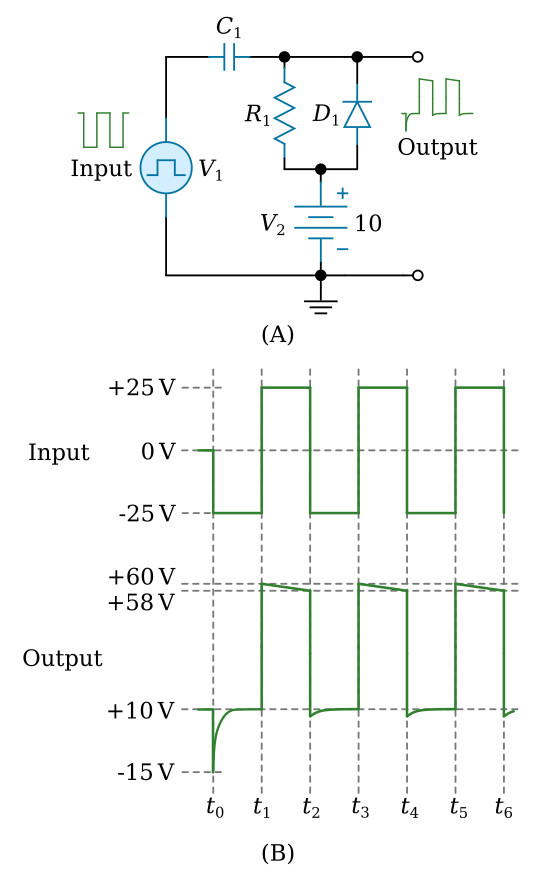
View A of the figure below is a positive clamper with negative bias. Observe that with no input signal, the capacitor charges through R1 to the bias battery voltage; the output voltage equals -10 volts. The circuit has negative bias because the positive side of the battery is grounded. The output waveform is shown in view B. Study the figure and waveforms carefully and note the following important points. Once again the peak-to-peak amplitude and shape of the output wave are, for all practical purposes, the same as the input wave. The lower extremity of the output wave is clamped to -10 volts, the value of the battery. Let's look at the circuit operation. The capacitor is initially charged to -10 volts with no input signal, and diode D1 does not conduct.
The -25 volt input signal provides forward bias for D1. The capacitor charges to +15 volts and retains most of its charge because its discharge through R1 is negligible. The +25 volt input signal is series aiding the capacitor voltage and develops +40 volts between the output terminals. When the input voltage is -25 volts, D1 conducts and the output voltage is -10 volts (-25 volts plus +15 volts). In this way the output reference is clamped at -10 volts. Changing the voltage of the battery changes the clamping reference level to the new voltage.