


Home > Textbooks > Basic Electronics > Amplifiers > Class B and AB Amplifiers >
Amplifiers
Class B and AB Amplifiers
Class A amplifiers described previously are usually used in equipments in which large power outputs are not required and high power efficiency is not a dominating factor. These amplifiers are used mainly in applications requiring minimum distortion. Class B push-pull power amplifiers are used mainly in equipments requiring high power output and high power efficiency.
Ideal Class B Amplifier
Let us look first at the ideal operation of this type of amplifier and then study the real operation of the push-pull circuit. The basic circuit of a class B push-pull amplifier is shown in the figure below. In this circuit, the input signal current introduces a voltage into the secondary winding of the transformer Tr1. One end of the secondary winding will become positive while the other end is going negative, when referred to the center-tap. Therefore, the input signal to the amplifier Q1 will be inverted in relation to the input signal to the amplifier Q2. This polarity inversion between the two exciting signals is necessary for proper operation of the push-pull amplifier. These two input signals should also be equal in magnitude. If interstage transformer coupling is undesirable, the transformer Tr1 may be replaced by one of the phase inverter circuits.
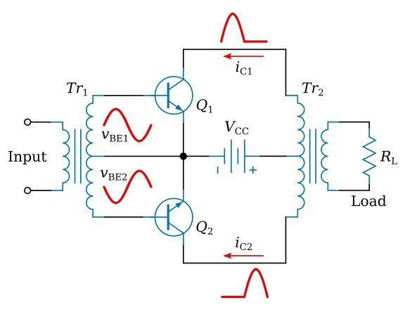
Since the input transformer Tr1 supplies two voltages of equal amplitude but 180 degrees out of phase when referred to the center-tap, one transistor is cut off while the other one is conducting. If the top transistor is conducting, current flows through the output transformer Tr2 in the direction of the collector of the upper transistor, through the transistor, and back through the battery in the center wire of the circuit. Little or no current flows in the lower half of the primary during this half-cycle period, because the lower transistor, in the off condition, acts like an open circuit. During the next half cycle, the top transistor is off, and the lower unit causes a current to flow through the lower part of the transformer, as shown in the figure above.
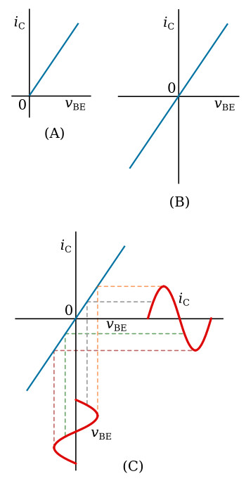
An indication of the output current waveform for a given input signal can be obtained by considering the dynamic transfer characteristic for the amplifier. This characteristic, for one of the transistors, is shown in view A of the figure above. The variations in output (collector) current is plotted against input (base) voltage under load conditions. Since two transistors are used, the overall dynamic transfer characteristic for the push-pull amplifier is obtained by placing two of the curves (view A of the figure above) back-to-back. The two curves are shown back-to-back and combined (view B of the figure above). In view C of the figure above, points on the input base voltage (a sine wave) are projected onto the dynamic transfer characteristic curve. The corresponding points are determined and projected as indicated to form the output collector current waveform.
As we can see in the figure above, if each transistor has a linear (ideal) transfer characteristic that starts at the origin, then with zero bias each transistor would have an output current consisting of a series of half-sine waves. The output transformer delivers a good sine wave of voltage to the load. Each transistor acts effectively as a half-wave amplifier and carries the total load for one-half of each cycle.
The major problem in a real version of class B push-pull circuit is crossover distortion. Since it is a real circuit, the transistors do not conduct when the base-to-emitter voltage is close to zero. As a result, the transfer characteristic for a single transistor is not a straight line passing through the origin. The input voltage must rise to approximately 0.7 V before the transfer characteristic becomes reasonably linear. Since this value is an appreciable part of the total driving voltage, a significant part of the output wave is clipped out of the center, as shown in the figure below.
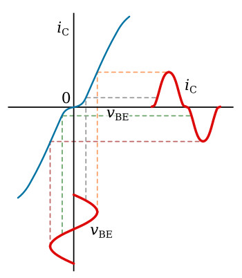
The crossover distortion becomes more severe with low signal input currents (voltages). This type of distortion can be eliminated by using a small forward bias on both transistors of the push-pull amplifier, resulting in class AB operation. With silicon transistors the amount of this bias is about 0.7 V.
Class AB Amplifier
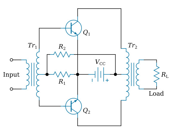
Since all transistor transfer functions have radical curvature in the low current region, class AB operation is usually preferable to class B. In class AB operation, the bases are biased to a voltage that causes a significant amount of collector current to flow in each transistor. A class AB push-pull circuit with the bias circuit is shown in the figure below. A voltage divider is formed by resistors R1 and R2. The voltage developed across resistor R1 supplies the base-emitter bias for both transistors. This small forward bias suppresses crossover distortion.
The bias voltage for class AB circuits can be adjusted so that the current flows for any period from 180 degrees to 360 degrees, giving modes of operation from just above class B operation to and including class A push-pull operation. Bias values close to class B are used for high efficiency, although class A conditions usually produce less overall distortion. Compromises may result in bias conditions between these two extremes.
By taking advantage of the fact that transistors are available in two polarities (NPN and PNP), a simple method of eliminating the need for an input transformer (or for a phase inverter) and for an output transformer is available. The resulting circuit is extremely simple, consisting of the parallel combination of a PNP and an NPN transistor (see the next section).


