


Home > Textbooks > Basic Electronics > Amplifiers > Phase Inverters >
Amplifiers
Phase Inverters
In an equipment, driver stages are located immediately before the power output stage. Push-pull stages require two input signals, each 180 degrees out of phase with the other. The phase requirement for the push-pull stage can be accomplished by using a tapped-secondary transformer between a single-ended (one transistor) driver stage and the output stage. For economy purposes and for better frequency response, transformer coupling may not be desirable. RC coupling normally is more economical and gives better frequency response.
If RC coupling is used between the driver stage and a push-pull stage, the driver stage must provide phase inversion to produce two signals 180 degrees out of phase. Phase inverters may use one stage (one transistor) or two stages (two transistors).
One-Stage Phase Inverters
The figure below shows a split-load phase inverter (transistor Q1) feeding a push-pull output stage (transistors Q2 and Q3, without biasing network).
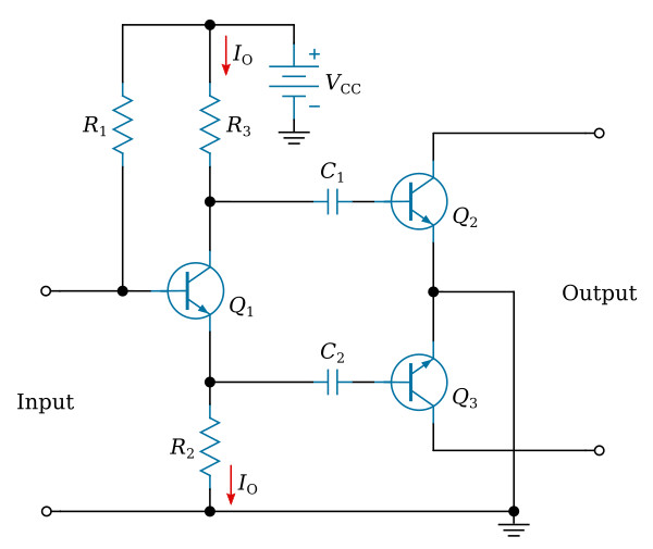
Output current of the transistor Q1 flows through collector load resistor R3 and emitter load resistor R2. Resistors R2 and R3 are equal in value. Resistor R1 establishes the base bias voltage.
When the input signal aids the forward bias (base becomes more positive), the output current (I0) increases. The increased output current causes the bottom side of resistor R3 to become less positive with respect to ground (top output signal decreases), and the top side of resistor R2 to become more positive with respect to ground (bottom output signal increases). When the input signal opposes the forward bias, the output current decreases and the top output signal from R3 increases, while the bottom output signal from R2 decreases. This action produces two output signals that are reversed 180 degrees with respect to each other. The signal developed across resistor R3 is coupled to the input circuit of transistor Q2 through DC blocking capacitor C1. The signal developed across resistor R2 is coupled to the input circuit of transistor Q3 through DC blocking capacitor C2.
In this circuit, equal voltage outputs are obtained by making resistor R2 equal in value to resistor R3. However, an unbalanced impedance results because the collector output impedance of transistor Q1 is higher than its emitter output impedance. Distortion can occur whenever strong signal current outputs occur.
The circuit in the figure below is similar to that shown in the figure above. However, the addition of resistor R4 overcomes the unbalanced output impedance. The functions of the parts in this circuit are the same as the correspondingly referenced parts in the unbalanced circuit.
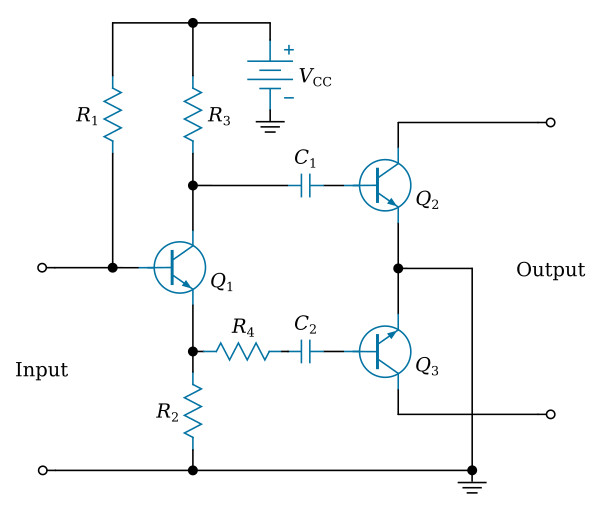
The values of resistors R2 and R4 are chosen so that the signal source impedance for transistor Q2 is equal to the signal source impedance for transistor Q3. This eliminates distortion at strong signal current values. The signal voltage loss across resistor R4 is compensated by making resistor R2 higher in value than resistor R3.
Because of the large negative feedback voltage developed across resistor R2, a large signal input is required to drive the one-stage phase inverter. This disadvantage can be overcome by using two-stage phase inverters. In addition, a two-stage phase inverter provides more power output than a one-stage phase inverter. This advantage is important if the driver stage must feed a large amount of power to a high-level push-pull power output stage.
Two-Stage Phase Inverter
The figure below shows a two-stage phase inverter consisting of two identical common-emitter configurations. Two signals, 180 degrees reversed in phase, are obtained from the phase inverter. Assume that an input signal drives the base of transistor Q1 negative. Because of the 180 degree phase reversal in the common-emitter configuration, the collector of transistor Q1 goes positive. One portion of this positive signal is coupled to the base of transistor Q2 through DC blocking capacitor C2 and attenuating resistor R4. The other portion of the positive signal is completed through DC blocking capacitor C4 to one input circuit of a push-pull output stage. The positive-going signal on the base of transistor Q2 causes a negative-going signal at the collector of transistor Q2. This negative signal is coupled through DC blocking capacitor C5 to the other input circuit of a push-pull output stage.
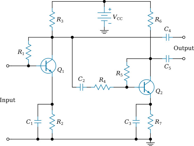
Resistor R1 provides base bias for transistor Q1. Collector load resistor R3 develops transistor Q1 output signal. Resistor R2 is the emitter swamping resistor and is AC bypassed by capacitor C1. Resistor R5 provides base bias for transistor Q2. Collector load resistor R6 develops transistor Q2 output signal. Resistor R7 is the emitter swamping resistor and is AC bypassed by capacitor C3.
Since two identical common-emitter configurations are used, the source impedances are equal for the two input circuits of the push-pull output stage. In addition, the amount of power that can be delivered by the two-stage phase inverter is much greater than that of the split-load phase inverter.


