


Home > Textbooks > Basic Electronics > Amplifiers > The Transistor Common Emitter Amplifier >
Amplifiers
The Transistor Common Emitter Amplifier
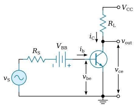
A basic transistor amplifier which has the emitter lead in common with the input and output circuits is shown below. The input voltage is between base and emitter and the output voltage between collector and emitter. The voltage VBB is introduced into the base circuit so that the emitter-base junction is forward-biased for control of the emitter-collector current. The base-to-emitter voltage is referred to as vbe and the base current as ib. The power supply voltage VCC is necessary to the circuit to make the collector positive with respect to the emitter and to provide a source for the output current. The collector-to-emitter voltage and collector current are vce and ic, respectively. The resistance RL is the load. The base current of the transistor controls the current through the collector and through the load resistor.
Output Characteristic Curves
Unfortunately, the resistance of the emitter and collector junctions of transistors are not always constant. Hence, Ohm's Law cannot always be used to express the relationship between the various currents and voltages in a transistor amplifier. For this and other reasons, this information is usually supplied by the manufacturer in graphical form. The figure below shows a graph of the collector (output) characteristics for the common emitter configuration of a transistor. The graph consists of a series of curves. Each curve shows, with the base current held constant, the collector current variation as the collector-to-emitter voltage is changed.
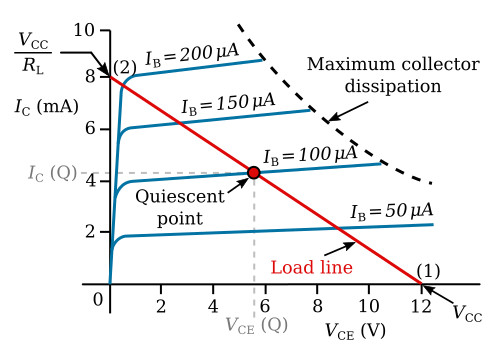
There are particular values for ib, vbe, ic, and vce even when no signal is applied to the input. The no-signal values of ib, vbe, ic, and vce are called the quiescent, or average, values and are given the symbols IB, VBE, IC, and VCE. The point defined by IC and VCE on the output characteristic curve is called the quiescent point (Q). The location of the quiescent point on the characteristic curve is an important part of the analysis of an amplifier circuit. The procedure is as follows: First a "load line" is determined for the values of supply voltage VCC and load resistance RL which are to be used in the amplifier circuit. Assume that ib is so small that the collector current ic = 0. If this were true, the voltage drop across RL would be zero and vce would equal VCC. This point 1 is plotted on the output characteristic curve (figure above). Then it is assumed that the base current is so large that the transistor becomes a perfect conductor so that vce = 0 and ic = VCC/RL. Plot this point 2 on the characteristic curve, and join points 1 and 2 with a straight line as in the figure above. This line is called the load line because it is determined only by the values of the load and VCC.
For the selected values of VCC and RL the resulting values of vce and ic must fall along the load line. The figure above, point Q, shows the no-signal values for VCE and IC as determined by the load line and the output characteristic for the selected average base current IB = 100 µA. The instantaneous base current ib depends on the sum of base bias current and input signal, and, by moving along the load line, the instantaneous values of vce and ic can be read from the graph for any given value of ib.
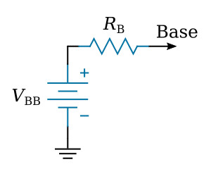
Note that the load line should fall well within the maximum collector-dissipation line. The maximum collector dissipation Pmax is a characteristic of the transistor and is usually given in the transistor manuals or catalog descriptions. The maximum collector-dissipation line is drawn by connecting all the points which satisfy the equation ICVCE = Pmax. The quiescent base current can be estimated by assuming that the base-to-emitter junction is simply the transistor input resistance hie. If vs = 0 (quiescent state), IB = VBB/(RS +hie). Often RS will be very much greater than hie so that IB ≈ VBB/RS. Thus the choice of bias voltage will depend on the nature of the signal source. Other methods of biasing will be discussed later.
Transistor Amplifier Characteristics
The change in vce or ic as a result of an input signal (a change in ib) could be determined by a graphical analysis of the characteristic curves as above for each value of ib. However, it is much more convenient to analyze the circuit mathematically after substituting an equivalent circuit for the transistor. It is not possible to derive a simple circuit which would replace the transistor for its entire operating range. This is because the characteristic curves of the transistor are not linear, as shown e.g. in the figure above. A linear equivalent circuit is only a valid approximation over small portions of the operating range. In other words, the equivalent circuit will not describe the relationship of the total quantities ib, vbe, ic, and vce, but it will describe the relationship of the small changes in these quantities. Equations for the various amplifier characteristics may be derived from the equivalent circuit and the mathematical relations used to obtain that circuit. Some of the characteristics (e.g. the voltage and current gains) of the common-emitter amplifier are given below. The actual derivations are not shown here.
The voltage gain could be approximated by the equation

where β is the transistor current gain and hie is the transistor input resistance in the common-emitter circuit. The minus sign indicates that the output voltage is 180° out of phase from the input voltage.
The current gain Ai is approximately
![]()
Again the minus sign is an indication of the phase reversal between the input and output signals.
The power gain Ap is simply the product of the current and voltage gains

The power gain does not include power losses in the signal source or in transferring the output signal to a load other than RL. It is simply the ratio of the signal power dissipated in RL to the signal power dissipated in the transistor input resistance hie.
The input resistance Rin is
![]()
The output resistance Rout could be approximated by the equation

where hoe is the conductance between the collector and emitter. As this equation indicates, the output resistance Rout is in this case the resistance that the transistor as a power source presents to the load RL. The output resistance of the entire amplifier circuit as seen by a device attached to the output terminals vce would actually be Rout in parallel with RL.
The common-emitter amplifier is thus shown to possess the properties of voltage gain, current gain, phase reversal of the input signal, low input resistance, and high output resistance.
Transistor Biasing
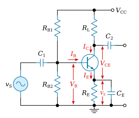
The use of a separate power source for the input and output circuits of the transistor amplifier is costly and inconvenient. Methods of providing the proper bias voltages from a single power source have, therefore, been devised. One of the most widely used bias systems is the voltage-divider type shown in the figure below (see the Types of Bias section for more info). Fixed bias is provided in this circuit by the voltage-divider network consisting of RB1, RB2, and the collector supply voltage (VCC). Resistor RE, which is connected in series with the emitter, provides the emitter with self-bias. A large capacitor bypassing RE will alleviate the loss in gain for AC signals.
Quiescent Point Determination
After it has been concluded that widely used transistor amplifiers could have a resistance in the emitter circuit and a voltage divider in the base, it is suitable to learn how to determine the quiescent point for such circuits. First, the load line is drawn in the usual way (see the graph of output characteristics above), care being taken to use RE + RL in calculating the current for VCE = 0. Now the circuit of figure above is redrawn considering the voltage divider as a series battery VBB and resistor RB (see Thevenin's theorem). It is first approximated that the emitter and the base have very nearly the same potential (VE = VB ≈ VBB) and that IE is very nearly IC. Therefore, IC ≈ VBB/RE. Looking at the load line to find the value of IB corresponding to this value of IC, one can improve on the approximation by correcting the base voltage to VBB - IBRB. Use this value of the base voltage to calculate a better value for IC. Usually this second approximation is sufficiently accurate.
Example of Transistor Bias Design
An example of how to go about determining reasonable resistance values for a transistor-amplifier circuit is given here. First, choose the desired quiescent point from the transistor's collector-characteristic curve. Evaluate from the characteristics or look up values for β, hie, and hoe in datasheets. Assume that, at the desired quiescent point (IC = 1 mA, VCE = 5 V), β = 55, hie = 2720 Ω, and hoe = 14 μS. Choose RL according to gain requirements and impedance matching, high values for current gain, moderate values for voltage gain with moderate output impedance. For this example RL = 25 kΩ. RB should be larger than hie to prevent excessive signal loss through the bias divider. Therefore, choose RB = 25 kΩ. For good stability choose RE = RB/5 = 5 kΩ. The required DC supply voltage is then (assuming IE ≐ IC)
![]()
The bias voltage VBB should equal the base voltage plus the voltage drop IBRB. VBB is thus


where VBE = 0.7 for silicon transistors. VBB can also be calculated as

Parallel combination of RB1 and RB2 is RB

Solving the two previous simultaneous equations for the bias resistors, RB1 = 142 kΩ and RB2 = 30.3 kΩ. The formulas derived previously for the voltage- and current-gain of the transistor amplifier apply also to this circuit. The amplifier output resistance is 1/hoe in parallel with RL. The amplifier input resistance is hie in parallel with RB.
Note: The current through the voltage divider RB1, RB2 should be at least 10 × IB. In our case the current through RB2


