Home > Textbooks > Basic Electronics > Amplifiers > Complementary Symmetry Circuit >
Amplifiers
Complementary Symmetry Circuit
Junction transistors are available as PNP and NPN types. If the two types of transistors are connected in a single stage (figure below), the current path (indicated by arrows) in the output circuit is completed through the collector-emitter junctions of the transistors. When connected in this manner, the circuit is referred to as a complementary symmetry circuit.
The complementary symmetry circuit provides all the advantages of conventional push-pull amplifiers without the need for a phase-inverter driver stage, or for a center-tapped input transformer. The parallel connection of the output circuit with respect to the load eliminates the need for a tapped-primary transformer in the output circuit.
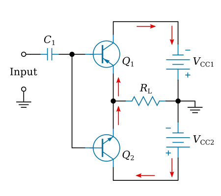
The figure above shows two transistors in a complementary symmetry connection. Transistor Q1 is a PNP transistor and transistor Q2 is an NPN transistor. A negative going input signal forward biases transistor Q1 and causes it to conduct. A positive going input signal forward biases transistor Q2 and causes it to conduct. As one transistor conducts, the other is nonconducting, because the signal that forward biases one transistor, reverse biases the other transistor.
The resultant action in the output circuit can be understood by considering the circuit of figure below. This is a simplified version of the output circuit. The internal emitter-collector circuit of transistor Q1 is represented by variable resistor R1 and that of transistor Q2 by variable resistor R2.
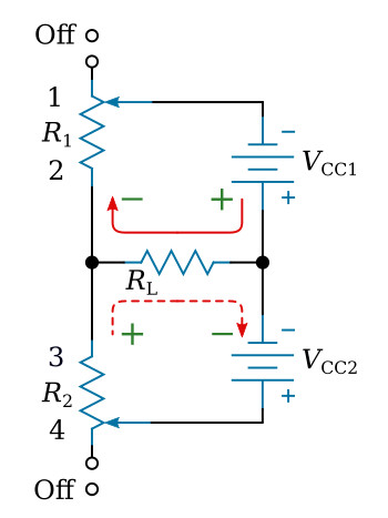
With no input signal and class B operation (zero emitter-base bias), the variable arms of the variable resistors can be considered to be in the Off positions (infinite resistances of R1 and R2). No current flows through the transistors nor through load resistor RL. As the incoming signal goes positive, transistor Q2 conducts and transistor Q1 remains nonconducting. Variable resistor R1 remains in the Off position. The variable arm of resistor R2 moves toward point 3 and current passes through the series circuit consisting of battery VCC2, variable resistor R2 and resistor RL. The amount of current flow depends upon the magnitude of the incoming signal, the variable arm moving toward point 3 for increasing forward bias and toward point 4 for decreasing forward bias. The current flows in the direction of the dashed arrow, producing a voltage with the indicated polarity. When the input signal goes negative, transistor Q1 conducts and transistor Q2 becomes nonconducting. The same action is repeated with variable resistor R1. Current flows through battery VCC1, load resistor RL, and variable resistor R1 in the direction shown by the solid-line arrow, and produces a voltage across resistor RL with the polarity indicated.
For class A operation of a complementary symmetry circuit, a voltage divider network (not shown) is used to apply forward bias to the two transistors so that collector current is not cut off at any time. In the simplified circuit (figure above), the variable resistors will not be in the Off position at any time. DC bias current in the output circuit flows out of the positive terminal of battery VCC2, through variable resistor R2, variable resistor R1, and into the negative terminal of battery VCC1. No current flows through resistor RL. Under these conditions, the output circuit can be considered a balanced bridge, the arms of the bridge consisting of resistors R1 and R2 and batteries VCC1 and VCC2. When the input signal goes positive, transistor Q2 conducts more and transistor Q1 conducts less. In the simplified circuit, the variable arm of resistor R1 moves toward point 1 and that of resistor R2 moves toward point 3. This action results in an unbalanced bridge and current flows through resistor RL in the direction of the dashed-line arrow, producing a voltage with the indicated polarity. When the input signal goes negative, transistor Q1 conducts more and transistor Q2 conducts less. In the simplified circuit, the variable arm of resistor R1 moves toward point 2 and that of resistor R2 moves toward point 4. Again the bridge is unbalanced, and current flows through resistor RL in the direction of the solid-line arrow, producing a voltage with the indicated polarity.
In either class B or class A, DC current does not flow through the load resistor. Advantage of this property can be taken by connecting the loudspeaker directly in place of resistor RL. The loudspeaker will not be offset by DC current flow through it and thus distortion will not occur.
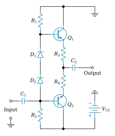
The figure below shows a complementary symmetry circuit to which a small forward bias has been applied. The voltage developed across diodes D1 and D2 provides forward bias for each transistor. The two diodes are chosen to match the characteristics of the transistors. R1 and R2 provide the necessary bias current and are usually made equal in order to bias both transistors equally.