


Home > Textbooks > Basic Electronics > Logic Gates > Direct-Coupled Transistor Logic (DCTL) >
Logic Gates
Direct-Coupled Transistor Logic (DCTL)
Transistorized digital circuits basically fulfill the three logical functions of AND (or NAND) gating, OR (or NOR) gating, and signal inversion (NOT gate). An additional function usually performed, though not logical in nature but nevertheless a practical necessity, is signal amplification. Other logical blocks, such as NOR, NAND, and flip-flops, are easily obtained using these three fundamental functional blocks. Several different circuit configurations can be used for these functional blocks. Normally these circuits are classified according to the elements used for interstage coupling or coupling between gates and inverters and amplifiers. The most commonly used coupling elements are diodes, resistors, resistor-capacitor combinations, and transistors themselves. It is also possible to design and use circuits without any of these coupling elements. Such circuits are referred to as direct-coupled transistor-logic circuits or, more commonly, DCTL. There are several advantages and some disadvantages of DCTL, and we consider these after discussing how this type of configuration works.
DCTL Inverters
The figure below shows three DCTL inverters in cascade. In this circuit the collector resistors R1, R2, and R3 serve as constant current sources. They supply current to their respective transistors' collectors, when they are on or to the base of the next transistor when they are off.
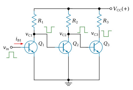
When the input voltage vin to the base of Q1 is near ground—that is at VCE(SAT) of the previous stage on transistor—voltage vC1 tends to approach the supply voltage VCC. Current is supplied to the base of Q2 through R1, and this turns Q2 on. The clamping action of the base-emitter diode of Q2 holds vC1 at the value determined by VBE2. Since Q2 is on, vC2 is now determined by the VCE(SAT) of Q2. If Q2 has a sufficiently low saturation drop, then vC2 will not be positive enough to turn Q3 on. The reverse situation holds true when a sufficiently positive voltage, vin, turns Q1 on. In this case vC1 will maintain Q2 off, which in turn will turn Q3 on. From this brief description several significant points are apparent. A low VCE(SAT) is a desirable feature of transistors used for DCTL. If the VCE(SAT) is high, then there is always the possibility that the next stage transistor may be erroneously turned on. Furthermore, in order to assure that all the fan-out transistors are held off, the VCE(SAT) must be smaller than the smallest VBE(ON) of the succeeding transistors. It is readily seen that the supply voltage can be relatively small because the output voltage swing varies between the VCE(SAT) of the on transistor and the VBE(ON) of the following stage transistors.
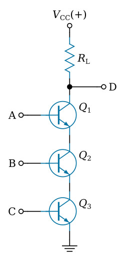
DCTL Series Gating
The figure below shows three transistors connected in series to form a NAND gate for positive input signals A, B, and C. If any of the three transistors is off, the output voltage at D will be the supply voltage (VCC) in the unloaded condition. Under loaded conditions, the voltage at D will depend on the resistor RL and the VBE(ON) of the next stage transistor. When all three transistors are on, the potential at D will be closer to ground than in the previous case and will be the sum of the VCE(SAT) of Q1, Q2, and Q3 in series. Consequently, the principal disadvantage of this configuration is the necessity to insure that the next stage transistor will be off when all three transistors are on. The sum of the three VCE(SAT) in series must be less than VBE(ON) of the next stage transistor. One means of accomplishing this is to supply more base drive to Q1, Q2, and Q3, thereby drawing them further into saturation and lowering the saturation resistance.
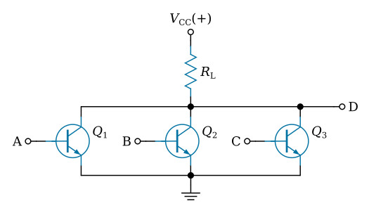
DCTL Parallel Gating
The figure below shows a parallel DCTL gate, which is really the previously considered "inverter" stage with three transistors having individual inputs instead of a single transistor. Obviously, this configuration is a NOR circuit. If any input is high on any of the three transistors, its collector will draw current through the load resistor, causing the output to go low.
Disadvantages of DCTL
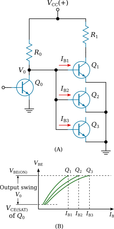
Current Hogging
One of the most undesirable features of DCTL is what is commonly known as
current hogging, and this phenomenon arises because of the spread in
VBE(ON) of the various driven (fan-out) transistors. No two
transistors will ever have identical input characteristics, and it is always
desirable to use transistors with as small a production spread as possible
on VBE(ON).
If the transistors Q1, Q2, and Q3 in the figure below (view A) have input characteristics as shown in the figure below (view B), it is quite clear that the output voltage swing V0 of transistor Q0 will be determined by the VCE(SAT) of Q0 and the VBE(ON) of one of the fan-out transistors. The figure below (view B) shows that the voltage V0 will be determined by the VBE(ON) of Q3, which will draw more current from R0 than either Q2 or Q1. It is quite possible that the unequal currents demanded by the fan-out transistors may result in some unit hogging more current and thereby starving the other transistors, which may not get sufficient base drive to saturate them, or in some cases, even turn them on at all.
The Crosstalk or the Noise Problem
In any high-speed system, pulses with fast rise times are likely to produce
potential differences in the ground system mainly because of ground inductances.
These voltages are likely to interfere with stable operation of the system.
DCTL systems are very susceptible to these noise voltages because the
operating and signal voltages are naturally low in these systems. If
several transistors on one end of a ground system are turned on, the
resulting pulse generated in the ground system can supply a positive
or negative pulse (depending on the polarity) which can cause faulty
turn-on or turn-off of other transistors further down the ground
system. One solution is to mount the transistors very close together,
thereby minimizing ground inductances. Besides ground noise, DCTL is also
vulnerable to noise on power supplies and stray noise picked up by connecting
leads. Of the various logic schemes, DCTL has one of the lowest noise margins,
typically 0.1 V at 125°C to about 0.2 V at room temperature, depending on
the fan-out and, whether the transistor is on or off.
Advantages of DCTL
In spite of its severe limitations, DCTL still has several desirable features. Since the voltage swings involved are small, transistors with relatively low breakdown ratings can be used. The fact that only one power-supply voltage is used is a very convenient feature. Since low voltages are used, sometimes as low as 3 volts, power dissipation in both the resistors and the transistors is quite low. Although DCTL systems are expensive in the number of transistors used, the absence of interstage coupling elements, different resistors sizes, clamping diodes, and many supply voltages make them relatively simple.


