


Home > Textbooks > Basic Electronics > Logic Gates > Transistor-Transistor Logic (TTL) >
Logic Gates
Transistor-Transistor Logic (TTL)
Transistor-transistor logic (TTL or T2L) integrated circuits were introduced in the late 1960s. TTL grew rapidly to be the most popular type of digital integrated circuit. Many improvements and variations have been added since its introduction. Today TTL continues to be a popular choice of integrated circuits.
TTL is best represented by the SN 54/74 series of digital integrated circuits. Texas Instruments Corporation originally developed this series of logic ICs but a number of manufacturers make them and use the same numbering system. The SN 54 (SN stands for semiconductor network) series is more expensive and designed for greater temperature range than the SN 74 series. The SN 54 devices will operate over a range of temperatures from -55 to +125 °C, whereas the SN 74 devices operate over a range from 0 to 70 °C. TTL ICs operate on a power supply voltage of 5 volts and require a well-regulated 5-volt power source. The most common IC packages available in TTL are the 14-pin or 16-pin dual-in-line package (DIP). Larger packages such as the 20-, 24-, and 28-pin DIPs usually consist of medium- or large-scale integrated circuits. The listing below indicates the different versions of TTL gates available, the power requirements per gate, propagation delay, and maximum operating speed.
| Version | Power per gate (mW) | Delay (ns) | Speed (MHz) |
|---|---|---|---|
| Standard SN 54/74 | 10 | 10 | 35 |
| High speed SN 54H/74H | 22 | 6 | 50 |
| Low power SN 54L/74L | 1 | 33 | 3 |
| Schottky SN 54S/74S | 20 | 3 | 125 |
| Low-power Schottky SN 54LS/74LS | 2 | 10 | 40 |
Analyzing the power and speed characteristics shows that if you want low power in a TTL IC, you will have to sacrifice speed and vice-versa.
A standard TTL logic gate is shown in the figure below. This gate performs the positive NAND function. Other TTL functions are implemented with this basic circuit or a modified version of it. The most important characteristics of a logic gate are speed and power consumption. These are the characteristics that are compared when logic circuits are evaluated. The standard TTL logic gate shown in the figure below has an average propagation delay time of 10 nanoseconds and a power dissipation of about 10 milliwatts.
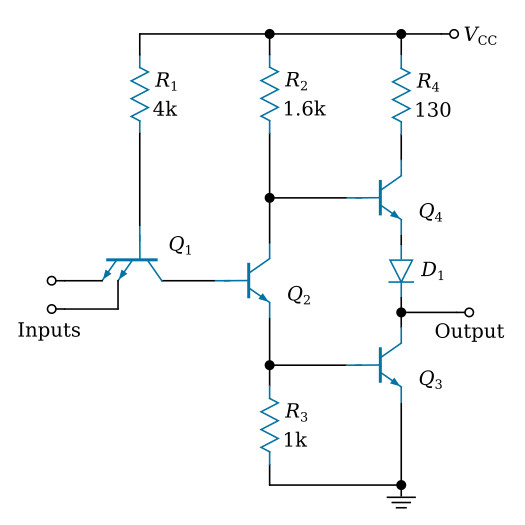
The TTL circuit, shown in the figure above, is analogous to the DTL (diode-transistor logic) circuit in certain respects. When TTL was developed, it made use of the economical feasibility of using transistors instead of diodes, and also solved the capacitive loading problem. The input transistor offers a significant advantage in switching time over the diode input of DTL. The addition of the phase-splitter driver and push-pull buffered-output circuit provides good noise rejection and excellent drive characteristics into capacitive loads.
Referring to the figure above, the TTL configuration employs a circuit which is a very low output impedance for high-capacity drive capability, high fan-out and good noise immunity. When the inputs of the circuit are high, Q2 and Q3 are driven "on" as common-emitter amplifiers. Transistor Q4 and its emitter diode are both lightly forward-biased but conduct only a negligible amount of current. When one of the inputs is low, Q2 and Q3 are both cut off, and Q4 conducts as an emitter-follower. The output is, therefore, pushed and pulled up and down by a transistor turning "on".
Schottky TTL (SN 54S/74S)
A significant improvement in speed of the basic TTL circuit was made by implementing it with Schottky transistors. A Schottky transistor is essentially a bipolar transistor which has a Schottky barrier or hot carrier diode connected between its base and collector as shown in view A of the figure below. This diode prevents the transistors in the TTL circuit from saturating and thereby, improves their ability to switch at higher speeds. View B of the figure below shows the symbol that is used to represent a Schottky transistor.
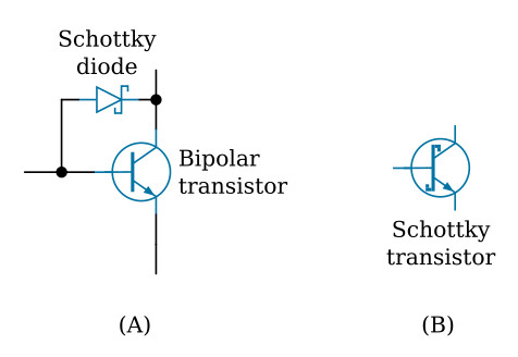
TTL logic circuits are saturating logic circuits. The transistors are switched between their cut off and saturated states. To saturate a bipolar transistor, a considerable amount of current must be supplied to the base of the transistor. The higher the base current, the faster the transistor saturates. High-based drive, however, slows down the turnoff of the transistor. It takes a finite period of time for the charge on the base to be removed before the transistor turns off. It is the one characteristic that most severely limits the switching speed of saturated logic circuits. The Schottky diode between the base and the collector of the bipolar transistor prevents saturation and, therefore, eliminates this problem. The Schottky diode switches very fast and requires only 0.1 to 0.3 volts of forward bias depending on temperature. When this diode is added, speed is increased because the time required to get a transistor out of saturation is not a factor. The diode will conduct before the transistor is allowed to saturate.
By using Schottky transistors and decreasing the values of the resistances in the standard TTL circuit, the speed of the basic TTL circuit can be greatly improved. A typical Schottky TTL gate circuit has a propagation delay of about 3 nanoseconds, which is less than one-third that of the standard TTL gate. This increased speed is obtained with an increase in power dissipation to about 20 milliwatts and, of course, the higher cost of the Schottky technique.
Low-Power Schottky TTL (SN 54LS/74LS)
A low-power version of the Schottky TTL gate is also available. This device uses much larger circuit resistances, thereby considerably reducing the power consumption. At the same time, Schottky transistors are used to improve the switching speed. A typical low-power Schottky TTL gate has a propagation delay of about 10 nanoseconds, with a power dissipation of 2 milliwatts. A low-power Schottky gate has the same propagation delay as a standard TTL gate, but its power dissipation is one-fifth of the standard gate. These improved speed-power characteristics are obtained at only a slight increase in cost over the standard circuit. At present, the low-power Schottky TTL circuit is perhaps the optimum TTL circuit. This accounts for its high popularity with digital designers.
Three-State TTL
Another TTL circuit widely used in computer applications is Tri-State (trademark of National Semiconductor) or three-state TTL. It is basically a standard TTL NAND gate with a third open or high impedance output state. A control input is used to effectively disconnect the circuit output from the IC pin (high impedance state). Three-state TTL circuits are used in bus-oriented digital circuit designs. A bus is a multiple conductor data path over which digital information is transmitted. In other words, a bus is a set of parallel transmission lines which are common to many digital circuits. The outputs and inputs of the digital circuits are connected to this common set of communication lines.
Open collector TTL
Standard TTL integrated circuits cannot be used to drive a data bus. Directly connecting the outputs of TTL circuits together will cause improper operation of the circuitry and, in some cases, cause damage to the circuits. The primary reason for the inability to use TTL circuits this way is the active pull-up transistor (Q4 in the standard TTL logic gate schematic shown in the figure above). This disadvantage has been overcome by making a variety of open collector TTL circuits available. Open collector TTL circuits do not contain the active pull-up transistor. The collector of the output inverter transistor is simply brought out to a pin on the integrated circuit and an external pull-up resistor is used. Open collector TTL circuit outputs can be connected directly together by using a simple pull-up resistor as shown in the figure below. We say that the circuit outputs are wired ORed. The gates not sending data on the bus line are controlled in such a way that their output is high and, therefore, the output inverter transistor is off. In this way the active circuit, that is, the circuit sending data on the bus line, can control whether that line is high or low.
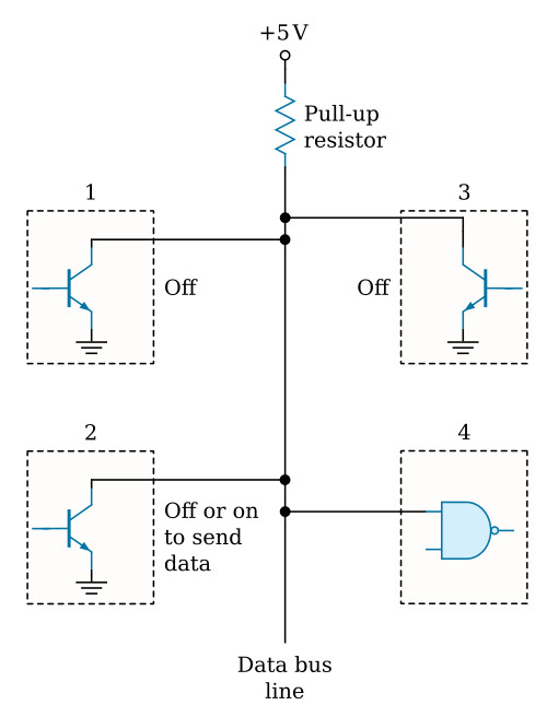
While open collector TTL circuits can be used in this way, many of the benefits of TTL circuits are lost by eliminating the active pull-up transistor. The high speed and high noise immunity associated with standard TTL circuits are lost when open collector circuits are used. To gain back these advantages and maintain the high speed and superior noise immunity of TTL circuits, the three-state TTL gate mentioned previously was developed.


