


Home > Textbooks > Basic Electronics > Logic Gates > Logic Families >
Logic Gates
Logic Families
Logic families are groups of logic circuits that are based on particular types of elements (resistors, transistors, and so forth). Families are identified by the manner in which the elements are connected, and, in some cases, by the types of elements used.
Logic circuits of a particular family can be interconnected without having to use additional circuitry. In other words, the output of one logic circuit can be used as the input to another logic circuit. This feature is known as compatibility. All circuits within a logic family will be compatible with the other circuits within that family.
Logic circuits are usually manufactured as integrated circuits and packaged in dual-inline (DIP) or other packages. Circuitry in a package is normally shown using standard logic symbols instead of individual components such as transistors, diodes, and so forth.
Several logic-circuit groups or families have been introduced. They differ primarily in the methods for carrying out the logic and the coupling to the inverter stages. For example, the transistor-transistor logic (TTL) uses a multiemitter transistor instead of the diodes found in DTL circuits. In emitter-coupled logic (ECL), the circuits are coupled by a common-emitter resistor, and complementary transistor logic (CTL) uses a combination of PNP and NPN transistors.
For each family, variations of a basic gate circuit are used to design a wide range of logic circuits with compatible input and output logical levels. In the design of a complete logic system, it is generally necessary to use logic circuits of one family only.
Before the various logic families are described, it is appropriate to discuss the general terminology used to describe logic families. These characteristics include logic assignments, logic voltage levels, supply voltage, noise margins, operating speeds, fan-in and fan-out, operating temperature, and power dissipation.
Logic Assignments
Two possible logic assignments, positive logic or negative logic, are used to implement a Boolean function. For positive logic, a logical "one" is represented by a "high" voltage level, and a logical "zero" is represented by a "low" voltage. The reverse is used to represent negative logic.
Logic Voltage Levels
Logic circuits are normally connected in cascade; that is, the output from one gate is connected to the input of the following gate, and so on. Thus, the switching behavior of one circuit depends not only on its own output characteristic, but may also depend on the input characteristic of the next gate. Consider the simple case of one inverter circuit driving another as shown in the figure below. With the second transistor disconnected, the output of Q1 will swing from VCE (saturated), about 0.1 volts, up to VCC (5 V). However, with the second stage connected, the positive voltage at the collector of Q1 will be limited to that of the base-emitter voltage of transistor Q2. Thus, the voltage swing at the output of transistor Q1 will now be from 0.1 to about 0.7 V
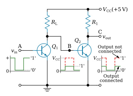
The output swing of transistor Q1, from 0.1 to 0.7 V, gives satisfactory operating points for the input of Q2, which in turn will give the same swing at its output when it is connected to the input of the next stage. The conditions for satisfactory switching between the two states are as follows: when Q1 is saturated, its collector voltage must be low enough to keep Q2 cut off; and when Q1 is cut off, the base current of Q2 (dependent on RL) must be high enough to saturate Q2.
For example, standard TTL voltage levels fix the logic 0 level between 0 and +0.8 V, while a logic 1 is between +2.4 and +5 V.
Supply Voltage
Integrated circuit manufacturers include the supply voltage limits of their digital circuits on the data sheets. For example, the correct operation of standard TTL circuits should fall between the 4.75 V and 5.25 V limits of the supply voltage. Within these limits, the device is designed to operate compatibly with the other TTL devices.
Noise Margin
In logic systems, the word noise refers to any unwanted voltage (AC or DC) appearing at the input of a logic circuit. If such a noise voltage were high enough, it could cause the circuit to change state with no change in the input signal voltage.
Both DC and AC noise should be considered in the design of digital systems. The DC noise is the steady drift in the voltage levels of the logic states, and AC noise is the narrow pulses that are created, primarily, by switching transients.
The DC noise margin (immunity) of a digital circuit is the ability of that circuit to maintain a logic state in the presence of DC noise. The DC noise margin is expressed by the following equations
![]()
![]()
where
NL - noise immunity of the digital circuit input when the
input signal is LOW,
NH - noise immunity of the digital circuit input when the input
signal is HIGH,
VILmax - maximum input voltage that can be read by the circuit
as LOW,
VOLmax - maximum output voltage that can represent LOW,
VOHmin - minimum output voltage than can represent HIGH,
VIHmin - minimum input voltage that can be read by the circuit
as HIGH.
Integrated circuit manufacturers include the voltage level limits of their digital circuits on the data sheets. From those values, the noise immunity can be computed.
For example, a standard TTL logic gate has the following
input and output level characteristics:
VILmax = 0.8 V, VOLmax = 0.4 V
VIHmin = 2 V, VOHmin = 2.4 V
Substituting these values into the noise immunity equations:
![]()
and
![]()
These values indicate that for reliable operation, the DC noise on the signal lines should not exceed 0.4 V.
It is relatively straightforward to specify the DC noise margin of a circuit, but this is not the whole story. Noise can appear at the input to a logic circuit as short, transient voltage pulses. The ability of a circuit to withstand such transient noise voltages is called the AC noise margin or AC noise immunity. The AC value therefore depends on the shape and duration of the voltage pulses, and may be affected by stray capacitances; the AC noise margin is much more difficult to define and specify.
Fan-in/Fan-out
Fan-out is the term used to describe the number of loads (inputs) that are driven from a single output. Sometimes it is necessary to better define the maximum fan-out capabilities of a circuit in terms of output current that can be supplied or sunk from a single output. For example, the maximum fan-out for a typical TTL gate is 10. This maximum fan-out reflects the ability of a single output to sink current from 10 identical gates at a logical "0" voltage, and to supply current to 10 identical gates at a logical "1" voltage level. In a typical TTL family this means that a single gate can sink a load current of 16 mA and supply a load current of 400 mA. Defining the maximum fan-out in terms of current is usually very important when interfacing two different families.
In summary, maximum fan-out of a single output is determined by the input-current requirements of the loads or circuits being driven, and is expressed in terms of equivalent devices that can be connected to a single output.
Note:
In some literature, the simpler term "fan-out" is used instead of the term
"maximum fan-out".
Fan-in is the number of inputs of a logic gate. Some devices provide increased fan-in by having provisions for the addition of expander circuits; fan-in also can be increased through combinational logic.
Operating Speed
It takes a finite time for a circuit to change from one logic state to the other. In a bipolar transistor, this time is that which is necessary for the base current to supply a charge to, or remove a charge from, the capacitive elements associated with the transistor structure, in order to produce the required voltage change at the output. In a circuit, additional time is required to charge any capacitance associated with the load. This time delay (between input and output) is called the propagation delay of the circuit. Delay values vary considerably depending on the particular circuit, but with integrated logic circuits the delay is typically in the range of 2 to 50 ns per gate. The overall propagation delay of a complete logic system will be the delay per gate multiplied by the number of gates in series.
An electric current is propagated along a wire at a rate of roughly 9 inches per ns. With discrete-component circuits, the time delay, due to the current traveling along the interconnecting wires, could be a significant part of the total circuit delay. However, with integrated circuits the interconnections are very short, and the time delay, due to current propagation, is usually negligible compared with the circuit delay.
Operating Temperature
All semiconductor devices are temperature sensitive. This is due primarily to the characteristics of the P-N junctions changing with temperature. Silicon transistors and diodes can operate satisfactorily with junction temperatures up to about 200° C; above this temperature the characteristics become so poor as to result in inferior performance. Resistors may also change their value with change of temperature due to the thermal generation of carriers and the change in the mobility of the carriers.
Power Dissipation
The power dissipation of a logic circuit is usually defined as the supply power required for the gate to operate with a 50 percent duty cycle, that is, equal times in the 0 and 1 logic states. The power dissipation of typical integrated logic circuits ranges from a few milliwatts to about 50 mW per gate, depending on the type of circuit. In general, high-speed circuits with short propagation delay require higher power.


